●Product Details
●The AD5330/AD5331/AD5340/AD5341 are single 8-/10-/12-bit DACs. They operate from a 2.5 V to 5.5 V supply consuming just 115 μA at 3 V and feature a power-down mode that further reduces the current to 80 nA. The devices incorporate an on-chip output buffer that can drive the output to both supply rails, but the AD5330, AD5340, and AD5341 allow a choice of buffered or unbuffered reference input.
●The AD5330/AD5331/AD5340/AD5341 have a parallel interface. CS selects the device and data is loaded into the input registers on the rising edge of WR.
●The GAIN pin allows the output range to be set at 0 V to VREF or 0 V to 2 × VREF.
●Input data to the DACs is double-buffered, allowing simultaneous update of multiple DACs in a system using the LDAC pin.
●An asynchronous CLR input is also provided, which resets the contents of the input register and the DAC register to all zeros. These devices also incorporate a power-on reset circuit that ensures that the DAC output powers on to 0 V and remains there until valid data is written to the device.
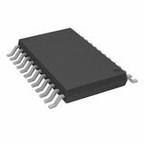
●The AD5330/AD5331/AD5340/AD5341 are available in thin shrink small outline packages (TSSOP).
●Applications
● Portable battery-powered instruments
● Digital gain and offset adjustment
● Programmable voltage and current sources
● Programmable attenuators
● Industrial process control
●### Features and Benefits
● Single 12-Bit DAC in 24-Lead TSSOP
● Low power operation: 115 μA @ 3 V, 140 μA @ 5 V
● Power-down to 80 nA @ 3 V, 200 nA @ 5 V via PD Pin
● 2.5 V to 5.5 V power supply
● Double-buffered input logic
● Guaranteed monotonic by design over all codes
● Buffered/unbuffered reference input options
● See Data Sheet for Additional Information

 Part 3D Model
