●Product Details
●The AD5663, a member of th _nano_DAC® family, is a low power, dual, 16-bit buffered voltage-out DAC that operates from a single 2.7 V to 5.5 V supply and is guaranteed monotonic by design.
●The AD5663 requires an external reference voltage to set the output range of the DAC. The part incorporates a power-on reset circuit that ensures the DAC output powers up to 0 V or midscale (AD5663BRMZ-1) and remains there until a valid write takes place. The part contains a power-down feature that reduces the current consumption of the device to 480 nA at 5 V and provides software-selectable output loads while in power-down mode.
●The low power consumption of this part in normal operation makes it ideally suited to portable, battery-operated equipment. The power consumption is 1.25 mW at 5 V, going down to 2.4 μW in power-down mode.
●The on-chip precision output amplifier of the AD5663 allows rail-to-rail output swing to be achieved.
●The AD5663 uses a versatile, 3-wire serial interface that operates at clock rates up to 50 MHz and is compatible with standard SPI®, QSPI™, MICROWIRE™, and DSP interface standards.
●Product Highlights
● 1. Dual 16-bit DAC; relative accuracy of ±12 LSBs maximum.
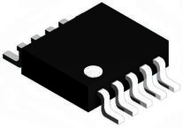
● 2. Available in 10-lead MSOP and 10-lead, 3 mm × 3 mm LFCSP_WD packages.
● 3. Low power; typically consumes 0.6 mW at 3 V and 1.25 mW at 5 V.
● 4. 7 μs maximum settling time.
●Applications
● Process control
● Data acquisition systems
● Portable battery-powered instruments
● Digital gain and offset adjustment
● Programmable voltage and current sources
● Programmable attenuators
●### Features and Benefits
● Low power, dual 16-bit nanoDAC
● Relative accuracy: ±12 LSBs maximum
● Guaranteed monotonic by design
● 10-lead MSOP and 3 mm × 3 mm LFCSP_WD
● 2.7 V to 5.5 V power supply
● Per channel power-down
● Power-on reset to zero scale or midscale
● Hardware LDAC and CLR functions
● Serial interface; up to 50 MHz

 Part 3D Model
