●Product Details
●The AD5791 is a single 20-bit, unbuffered voltage-output DAC that operates from a bipolar supply of up to 33 V. The AD5791 accepts a positive reference input in the range 5 V to VDD – 2.5V and a negative reference input in the range VSS + 2.5 V to 0 V. The AD5791 offers a relative accuracy specification of ±1 LSB max, and operation is guaranteed monotonic with a ±1 LSB DNL max specification.
●The part uses a versatile 3-wire serial interface that operates at clock rates up to 35 MHz and that is compatible with standard SPI, QSPI™, MICROWIRE™, and DSP interface standards. The part incorporates a power-on reset circuit that ensures the DAC output powers up to 0 V and in a known output impedance state and remains in this state until a valid write to the device takes place. The part provides an output clamp feature that places the output in a defined load state.
●Product Highlights
● 1. 1 ppm Accuracy.
● 2. Wide Power Supply Range up to ±16.5 V.
● 3. Operating Temperature Range: −40°C to +125°C.
● 4. Low 7.5 nV/√Hz Noise Spectral Density.
● 5. Low 0.05 ppm/°C Temperature Drift.
●Applications
● Medical Instrumentation
● Test and Measurement
● Industrial Control
● High end Scientific and Aerospace Instrumentation
●### Features and Benefits
● 1-ppm Resolution
● 1-ppm INL
● 7.5nV/√Hz Noise Spectral Density
● 0.19 LSB long term linearity stability
● <0.05 ppm/°C temperature drift
● 1μs Settling Time
● 1.4 nV-sec glitch impulse
● Operating temperature range:
●-40°C to 125°C
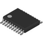
● 20-Lead TSSOP package
● Wide Power Supply Range up to ±16.5 V
● 35 MHz Schmitt Triggered Digital Interface
● 1.8 V compatible digital interface
●AD5791-EP supports defense and aerospace applications (AQEC standard)
● Download the AD5791-EP Data Sheet (pdf)
● Military temperature range (−55°C to +125°C)
● Controlled manufacturing baseline
● One assembly/test site
● One fabrication site
● Enhanced product change notification
● Qualification data available on request
● V62/12664 DSCC Drawing Number

 Part 3D Model
