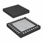
●Product Details
●The AD6677 is an 11-bit, 250 MSPS, intermediate frequency (IF) receiver specifically designed to support multi-antenna systems in telecommunication applications where high dynamic range performance, low power, and small size are desired.
●The device consists of a high performance analog-to-digital converter (ADC) and a noise shaping requantizer (NSR) digital block. The ADC consists of a multistage, differential pipelined architecture with integrated output error correction logic, and each ADC features a wide bandwidth switched capacitor sampling network within the first stage of the differential pipeline. An integrated voltage reference eases design considerations. A duty cycle stabilizer (DCS) compensates for variations in the ADC clock duty cycle, allowing the converters to maintain excellent performance.
●The ADC output is connected internally to an NSR block. The integrated NSR circuitry allows for improved SNR performance in a smaller frequency band within the Nyquist bandwidth. The device supports two different output modes selectable via the SPI. With the NSR feature enabled, the output of the ADC are processed such that the AD6677 supports enhanced SNR performance within a limited portion of the Nyquist bandwidth while maintaining an 11-bit output resolution.
●The NSR block can be programmed to provide a bandwidth of either 22% or 33% of the sample clock. For example, with a sample clock rate of 250 MSPS, the AD6677 can achieve up to 76.3 dBFS SNR for a 55 MHz bandwidth in the 22% mode and up to 73.5 dBFS SNR for a 82 MHz bandwidth in the 33% mode.
●When the NSR block is disabled, the ADC data is provided directly to the output at a resolution of 11 bits. The AD6677 can achieve up to 65.9 dBFS SNR for the entire Nyquist bandwidth when operated in this mode. This allows the AD6677 to be used in telecommunication applications such as a digital predistortion observation path where wider bandwidths are required.
●The output data is routed directly to an external JESD204B serial output lane. This output is at current mode logic (CML) voltage levels. One mode is supported such that the output coded data is sent through one lane (L = 1; F = 4). Synchronization input controls (SYNCINB± and SYSREF±) are provided.
●The AD6677 receiver digitizes a wide spectrum of IF frequencies. This IF sampling architecture greatly reduces component cost and complexity compared with traditional analog techniques or less integrated digital methods.
●Flexible power-down options allow significant power savings, when desired. Programmable overrange level detection is supported via dedicated fast detect pins.
●Product Highlights
● 1. The configurable JESD204B output block with an integrated phase-locked loop (PLL) to support lane rates up to 5 Gbps.
● 2. IF receiver includes an 11-bit, 250 MSPS ADC with programmable noise shaping requantizer (NSR) function that allows for improved SNR within a reduced bandwidth of 22% or 33% of the sample rate.
● 3. Support for an optional RF clock input to ease system board design.
● 4. Proprietary differential input maintains excellent SNR performance for input frequencies of up to 400 MHz.
● 5. An on-chip integer, 1 to 8 input clock divider and SYNC input allows synchronization of multiple devices.
● 6. Operation from a single 1.8 V power supply.
● 7. Standard serial port interface (SPI) that supports various product features and functions, such as controlling the clock DCS, power-down, test modes, voltage reference mode, overrange fast detection, and serial output configuration.
●Applications
● Communications
● Diversity radio and smart antenna (MIMO) systems
● Multimode digital receivers (3G)
●TD-SCDMA, WiMAX, WCDMA,
●CDMA2000, GSM, EDGE, LTE
● I/Q demodulation systems
● General-purpose software radios
●### Features and Benefits
● JESD204B Subclass 0 or Subclass 1 coded serial digital outputs
● Signal-to-noise ratio (SNR) = 71.9 dBFS at 185 MHz AIN and 250 MSPS with NSR set to 33%
● Spurious-free dynamic range (SFDR) = 87 dBc at 185 MHz AIN and 250 MSPS
● Total power consumption:
●435 mW at 250 MSPS
● 1.8 V supply voltages
● Integer 1 to 8 input clock divider
● Sample rates of up to 250 MSPS
● IF sampling frequencies of up to 400 MHz
● Internal analog-to-digital converter (ADC) voltage reference
● Flexible analog input range
●1.4 V p-p to 2.0 V p-p (1.75 V p-p nominal)
● ADC clock duty cycle stabilizer (DCS)
● Serial port control
● Energy saving power-down modes

 Part 3D Model
