●Product Details
●The AD9508 provides clock fanout capability in a design that emphasizes low jitter to maximize system performance. This device benefits applications like clocking data converters with demanding phase noise and low jitter requirements.
●There are four independent differential clock outputs, each with various types of logic levels available. Available logic types include LVDS (1.65 GHz), HSTL (1.65 GHz), and 1.8 V CMOS (250 MHz). In 1.8 V CMOS output mode, the differential output becomes two CMOS single-ended signals. The CMOS outputs are 1.8 V logic levels, regardless of the operating supply voltage.
●Each output has a programmable divider that can be bypassed or be set to divide by any integer up to 1024. In addition, the AD9508 supports a coarse output phase adjustment between the outputs.
●The device can also be pin programmed for various fixed configurations at power-up without the need for SPI or I2C programming.
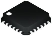
●The AD9508 is available in a 24-lead LFCSP and operates from a either a single 2.5 V or 3.3 V supply. The temperature range is −40°C to +85°C.
●Applications
● Low jitter, low phase noise clock distribution
● Clocking high speed ADCs, DACs, DDSs, DDCs, DUCs, MxFEs
● High performance wireless transceivers
● High performance instrumentation
● Broadband infrastructure
●### Features and Benefits
● 1.65 GHz differential clock inputs/outputs
● 10-bit programmable dividers, 1 to 1024, all integers
● Up to 4 differential outputs or 8 CMOS outputs
● Pin strapping capability for hardwired programming at power-up
● <115 fs rms broadband random jitter
● Additive output jitter: 41 fs rms typical (12 kHz to 20 MHz)
● Excellent output-to-output isolation
● Automatic synchronization of all outputs
● See data sheet for additional features
●AD9508-EP supports defense and aerospace applications (AQEC standard)
● Download AD9508-EP data sheet (pdf)
● Extended temperature range: −55°C to +105°C
● Controlled manufacturing baseline
● One assembly/test site
● One fabrication site
● Enhanced product change notification
● Qualification data available on request
● V62/13626 DSCC Drawing Number

 Part 3D Model
