●Product Details
●The AD9656 is a quad, 16-bit, 125 MSPS analog-to-digital converter (ADC) with an on-chip sample and hold circuit designed for low cost, low power, small size, and ease of use. The device operates at a conversion rate of up to 125 MSPS and is optimized for outstanding dynamic performance and low power in applications where a small package size is critical.
●The ADC requires a single 1.8 V power supply and LVPECL-/CMOS-/LVDS-compatible sample rate clock for full performance operation. An external reference or driver components are not required for many applications.
●Individual channel power-down is supported and typically consumes less than 14 mW when all channels are disabled. The ADC contains several features designed to maximize flexibility and minimize system cost, such as a programmable output clock, data alignment, and digital test pattern generation. The available digital test patterns include built-in deterministic and pseudo-random patterns, along with custom user-defined test patterns entered via the serial port interface (SPI).
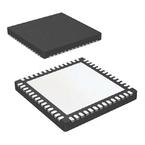
●The AD9656 is available in an RoHS compliant, nonmagnetic, 56-lead LFCSP. It is specified over the −40°C to +85°C industrial temperature range.
● Product Highlights
● 1. It has a small footprint. Four ADCs are contained in a small, 8 mm × 8 mm package.
● 2. An on-chip phase-locked loop (PLL) allows users to provide a single ADC sampling clock; the PLL multiplies the ADC sampling clock to produce the corresponding JESD204B data rate clock.
● 3. The configurable JESD204B output block supports up to 8.0 Gbps per lane.
● 4. JESD204B output block supports one, two, and four lane configurations.
● 5. Low power of 198 mW per channel at 125 MSPS, two lanes.
● 6. The SPI control offers a wide range of flexible features to meet specific system requirements.
●Applications
● Medical imaging
● High speed imaging
● Quadrature radio receivers
● Diversity radio receivers
● Portable test equipment
●### Features and Benefits
● SNR = 79.9 dBFS at 16 MHz (VREF = 1.4 V)
● SNR = 78.1 dBFS at 64 MHz (VREF = 1.4 V)
● SFDR = 86 dBc to Nyquist (VREF = 1.4 V)
● JESD204B Subclass 1 coded serial digital outputs
● Flexible analog input range: 2.0 V p-p to 2.8 V p-p
● 1.8 V supply operation
● Low power: 197 mW per channel at 125 MSPS (two lanes)
● DNL = ±0.6 LSB (VREF = 1.4 V)
● INL = ±4.5 LSB (VREF = 1.4 V)
● 650 MHz analog input bandwidth, full power
● Serial port control
● Full chip and individual channel power-down modes
● Built-in and custom digital test pattern generation
● Multichip sync and clock divider
● Standby mode
 Part 3D Model
