●Product Details
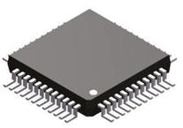
●The AD9763/AD9765/AD9767 are dual-port, high speed, 2-channel, 10-/12-/14-bit CMOS DACs. Each part integrates two high quality TxDAC+® cores, a voltage reference, and digital interface circuitry into a small 48-lead LQFP. The AD9763/ AD9765/AD9767 offer exceptional ac and dc performance while supporting update rates of up to 125 MSPS.
●The AD9763/AD9765/AD9767 have been optimized for processing I and Q data in communications applications. The digital interface consists of two double-buffered latches as well as control logic. Separate write inputs allow data to be written to the two DAC ports independent of one another. Separate clocks control the update rate of the DACs.
●A mode control pin allows the AD9763/AD9765/AD9767 to interface to two separate data ports, or to a single interleaved high speed data port. In interleaving mode, the input data stream is demuxed into its original I and Q data and then latched. The I and Q data is then converted by the two DACs and updated at half the input data rate.
●The GAINCTRL pin allows two modes for setting the full-scale current (IOUTFS) of the two DACs. IOUTFS for each DAC can be set independently using two external resistors, or IOUTFS for both DACs can be set by using a single external resistor. See the Gain Control Mode section for important date code information on this feature.
●The DACs utilize a segmented current source architecture combined with a proprietary switching technique to reduce glitch energy and maximize dynamic accuracy. Each DAC provides differential current output, thus supporting single-ended or differential applications. Both DACs of the AD9763, AD9765, or AD9767 can be simultaneously updated and can provide a nominal full-scale current of 20 mA. The full-scale currents between each DAC are matched to within 0.1%.
●The AD9763/AD9765/AD9767 are manufactured on an advanced, low cost CMOS process. They operate from a single supply of 3.3 V to 5 V and consume 380 mW of power.
●Product Highlights
● 1. The AD9763/AD9765/AD9767 are members of a pin- compatible family of dual TxDACs providing 8-, 10-, 12-, and 14-bit resolution.
● 2. Dual 10-/12-/14-Bit, 125 MSPS DACs. A pair of high performance DACs for each part is optimized for low distortion performance and provides flexible transmission of I and Q information.
● 3. Matching. Gain matching is typically 0.1% of full scale, and offset error is better than 0.02%.
● 4. Low Power. Complete CMOS dual DAC function operates on 380 mW from a 3.3 V to 5 V single supply. The DAC full-scale current can be reduced for lower power operation, and a sleep mode is provided for low power idle periods.
● 5. On-Chip Voltage Reference. The AD9763/AD9765/AD9767 each include a 1.20 V temperature-compensated band gap voltage reference.
● 6. Dual 10-/12-/14-Bit Inputs. The AD9763/AD9765/AD9767 each feature a flexible dual-port interface, allowing dual or interleaved input data.
●Applications
● Communications
● Base stations
● Digital synthesis
● Quadrature modulation
● 3D ultrasound
●### Features and Benefits
● 10-/12-/14-bit dual transmit digital-to-analog converters (DACs)
● 125 MSPS update rate
● Excellent SFDR to Nyquist @ 5 MHz output: 75 dBc
● Excellent gain and offset matching: 0.1%
● Fully independent or single-resistor gain control
●|
● Dual-port or interleaved data
● On-chip 1.2 V reference
● 5 V or 3.3 V operation
● Power dissipation: 380 mW @ 5 V
● Power-down mode: 50 mW @ 5 V
● 48-lead LQFP
●---|---

 Part 3D Model
