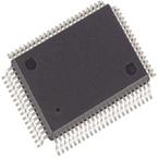
●Product Details
●The AD9775 is the 14-bit member of the AD977x pin-compatible, high performance, programmable 2×/4×/8× interpolating TxDAC+ family. The AD977x family features a serial port interface (SPI) that provides a high level of programmability, thus allowing for enhanced system-level options. These options include selectable 2×/4×/8× interpolation filters; fS/2, fS/4, or fS/8 digital quadrature modulation with image rejection; a direct IF mode; programmable channel gain and offset control; programmable internal clock divider; straight binary or twos complement data interface; and a single-port or dual-port data interface.
●The selectable 2×/4×/8× interpolation filters simplify the requirements of the reconstruction filters while simultaneously enhancing the pass-band noise/distortion performance of TxDAC+ devices. The independent channel gain and offset adjust registers allow the user to calibrate LO feedthrough and sideband suppression errors associated with analog quadrature modulators. The 6 dB of gain adjustment range can also be used to control the output power level of each DAC.
●The AD9775 can perform fS/2, fS/4, and fS/8 digital modulation and image rejection when combined with an analog quadrature modulator. In this mode, the AD9775 accepts I and Q complex data (representing a single or multicarrier waveform), generates a quadrature modulated IF signal along with its orthogonal representation via its dual DACs, and presents these two reconstructed orthogonal IF carriers to an analog quadrature modulator to complete the image rejection upconversion process. Another digital modulation mode (that is, the direct IF mode) allows the original baseband signal representation to be frequency translated such that pairs of images fall at multiples of one-half the DAC update rate.
●The AD977x family includes a flexible clock interface that accepts differential or single-ended sine wave or digital logic inputs. An internal PLL clock multiplier is included and generates the necessary on-chip high frequency clocks. It can also be disabled to allow the use of a higher performance external clock source. An internal programmable divider simplifies clock generation in the converter when using an external clock source. A flexible data input interface allows for straight binary or twos complement formats and supports single-port interleaved or dual-port data.
●Dual high performance DAC outputs provide a differential current output programmable over a 2 mA to 20 mA range.
●The AD9775 is manufactured on an advanced 0.35 micron CMOS process, operates from a single supply of 3.1 V to 3.5 V, and consumes 1.2 W of power.
●Product Highlights
● 1. The AD9775 is the 14-bit member of the AD977x pin-compatible, high performance, programmable 2×/4×/8× interpolating TxDAC+ family.
● 2. Direct IF transmission capability for 70 MHz + IFs through a novel digital mixing process.
● 3. fS/2, fS/4, and fS/8 digital quadrature modulation and user-selectable image rejection to simplify/remove cascaded SAW filter stages.
● 4. A 2×/4×/8× user-selectable, interpolating filter eases data rate and output signal reconstruction filter requirements.
● 5. User-selectable, twos complement/straight binary data coding.
● 6. User-programmable, channel gain control over 1 dB range in 0.01 dB increments.
● 7. User programmable channel offset control ±10% over the FSR.
● 8. Ultrahigh speed 400 MSPS DAC conversion rate.
●### Features and Benefits
● 14-bit resolution, 160 MSPS/400 MSPS input/output data rate
● Selectable 2×/4×/8× interpolating filter
● Programmable channel gain and offset adjustment
● fS/4, fS/8 digital quadrature modulation capability
● Direct IF transmission mode for 70 MHz + IFs
● Enables image rejection architecture
● Fully compatible SPI® port
● Excellent ac performance
●SFDR: −71 dBc @ 2 MHz to 35 MHz W-CDMA
●ACPR: −71 dB @ IF = 19.2 MHz
● Internal PLL clock multiplier
● Selectable internal clock divider
● Versatile clock input
● Differential/single-ended sine wave or TTL/CMOS/LVPECL compatible


