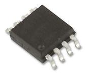
●Product Details
●The ADA4622-1/ADA4622-2 are the next generation of the AD820 and the AD822 single-supply, rail-to-rail output (RRO), precision junction field effect transistors (JFET) input op amps. The ADA4622-1/ADA4622-2 include many improvements that make them desirable as an upgrade without compromising the flexibility and ease of use that makes the AD820 and the AD822 useful for a wide variety of applications.
●The input voltage range includes the negative supply and the output swings rail-to-rail. Input EMI filters increase the signal robustness in the face of closely located switching noise sources.
●The speed, in terms of bandwidth and slew rate, increases along with a strong output drive to improve settling time performance and enable the devices to drive the inputs of modern single-ended, successive approximation register (SAR) analog-to-digital converters (ADCs).
●Voltage noise is reduced; while keeping the supply current the same as the AD820 and the AD822, broadband noise is reduced by 25%, and 1/f is reduced by half. DC precision in the ADA4622-1/ADA4622-2 improved from the AD820 and the AD822 with half the offset and a maximum thermal drift specification added to the ADA4622-1/ADA4622-2. The common-mode rejection ratio (CMRR) is improved from the AD820 and the AD822 to make the ADA4622-1/ADA4622-2 more suitable when used in noninverting gain and difference amplifier configurations.
●The ADA4622-1/ADA4622-2 are specified for operation over the extended industrial temperature range of −40°C to +125°C and operates from 5 V to 30 V with specifications at +5 V, ±5 V, and ±15 V. The ADA4622-1 is available in a 5-lead SOT-23 package and an 8-lead LFCSP package, and the ADA4622-2 is available in an 8-lead SOIC package, an 8-lead MSOP package, and an 8-lead LFCSP package.
●Applications
● High output impedance sensor interfaces
● Photodiode sensor interfaces
● Transimpedance amplifiers
● ADC drivers
● Precision filters and signal conditioning
●### Features and Benefits
● Next generation of the AD820/AD822
● Wide gain bandwidth product: 8 MHz typical
● High slew rate: +23 V/μs/−18 V/μs typical
● Low input bias current: ±10 pA maximum at TA = 25°C
● Low offset voltage
● A grade: ±0.8 mV maximum at TA = 25°C
● B grade: ±0.35 mV maximum at TA = 25°C
● Low offset voltage drift
● A grade: ±2 μV/°C typical, ±15 μV/°C maximum
● B grade: ±2 μV/°C typical, ±5 μV/°C maximum
● Input voltage range includes Pin V−
● Rail-to-rail output
● Electromagnetic interference rejection ratio (EMIRR)
● 90 dB typical at f = 1000 MHz and f = 2400 MHz
● Industry-standard package and pinouts

 Part 3D Model
