●Product Details
●The ADA4950-1/ADA4950-2 are gain-selectable versions of the ADA4932-1/ADA4932-2 with on-chip feedback and gain resistors It is an ideal choice for driving high performance ADCs as a single-ended-to-differential or differential-to-differential amplifier. The output common-mode voltage is user adjustable by means of an internal common-mode feedback loop, allowing the ADA4950-x output to match the input of the ADC. The internal feedback loop also provides exceptional output balance as well as suppression of even-order harmonic distortion products.
●Differential gain configurations of 1, 2, and 3 are easily realized with internal feedback networks that are connected externally to set the closed-loop gain of the amplifier.
●The ADA4950-x is fabricated using the Analog Devices, Inc., proprietary silicon-germanium (SiGe) complementary bipolar process, enabling it to achieve low levels of distortion and noise at low power consumption. The low offset and excellent dynamic performance of the ADA4950-x make it well suited for a wide variety of data acquisition and signal processing applications.
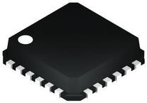
●The ADA4950-x is available in a Pb-free, 3 mm × 3 mm, 16-lead LFCSP (ADA4950-1, single) or a Pb-free 4 mm × 4 mm, 24-lead LFCSP (ADA4950-2, dual). The pinout has been optimized to facilitate PCB layout and minimize distortion. The ADA4950-1/ADA4950-2 are specified to operate over the -40°C to +105°C temperature range; both operate on supplies from +3 V to ±5 V.
●Applications
● ADC drivers
● Single-ended-to-differential converters
● IF and baseband gain blocks
● Differential buffers
● Line drivers
●### Features and Benefits
● High performance at low power
● High speed
●-3 dB bandwidth of 750 MHz, G = 1
●0.1 dB flatness to 210 MHz, VOUT, dm = 2 V p-p, RL, dm = 200 Ω
●Slew rate: 2900 V/µs, 25% to 75%
●Fast 0.1% settling time of 9 ns
● Low power: 9.5 mA per amplifier
● Low harmonic distortion
●108 dB SFDR @ 10 MHz
●98 dB SFDR @ 20 MHz
● Low output voltage noise: 9.2 nV/√Hz, G = 1, RTO
● ±0.2 mV typical input offset voltage
● Selectable differential gains of 1, 2, and 3
● Differential-to-differential or single-ended-to-differential operation
● Adjustable output common-mode voltage
● Input common-mode range shifted down by one VBE
● Wide supply range: +3 V to ±5 V
● Available in 16-lead and 24-lead LFCSP packages

 Part 3D Model
