●Product Details
●The ADCMP609 is a fast comparator fabricated on XFCB2, an Analog Devices, Inc., proprietary process. These comparators are exceptionally versatile and easy to use. Features include an input range from VEE − 0.2 V to VCC \+ 0.2 V, low noise, TTL-/CMOS-compatible output drivers, and adjustable hysteresis and/or shutdown inputs.
●The device offers 40 ns propagation delay driving a 15 pF load with 10 mV overdrive on 500 μA typical supply current.
●A flexible power supply scheme allows the devices to operate with a single +2.5 V positive supply and a −0.2 V to +3.0 V input signal range up to a +5.5 V positive supply with a −0.2 V to +5.7 V input signal range.
●The TTL-/CMOS-compatible output stage is designed to drive up to 15 pF with full rated timing specifications and to degrade in a graceful and linear fashion as additional capacitance is added. The input stage of the comparator offers robust protection against large input overdrive, and the outputs do not phase reverse when the valid input signal range is exceeded. A programmable hysteresis feature is also provided.
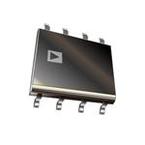
●The ADCMP609, available in an 8-lead MSOP package, features a shutdown pin and hysteresis control.
●Applications
● High speed instrumentation
● Clock and data signal restoration
● Logic level shifting or translation
● High speed line receivers
● Threshold detection
● Peak and zero-crossing detectors
● High speed trigger circuitry
● Pulse-width modulators
● Current-/voltage-controlled oscillators
●Data Sheet, Rev. A, 8/07
●### Features and Benefits
● Fully specified rail-to-rail at VCC = 2.5 V to 5.5 V
● Input common-mode voltage from −0.2 V to VCC \+ 0.2 V
● Low glitch TTL-/CMOS-compatible output stage
● 40 ns propagation delay
● Low power 1 mW at 2.5 V
● Shutdown pin
● Programmable hysteresis
● Power supply rejection > 60 dB
● −40°C to +125°C operation

 Part 3D Model
