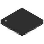
●Product Details
●The ADF4193 frequency synthesizer can be used to implement local oscillators in the upconversion and downconversion sections of wireless receivers and transmitters. Its architecture is specifically designed to meet the GSM/EDGE lock time requirements for base stations. It consists of a low noise, digital phase frequency detector (PFD), and a precision differential charge pump. There is also a differential amplifier to convert the differential charge pump output to a single-ended voltage for the external voltage-controlled oscillator (VCO).
●The Σ-Δ-based fractional interpolator, working with the N divider, allows programmable modulus fractional-N division. Additionally, the 4-bit reference (R) counter and on-chip frequency doubler allow selectable reference signal (REFIN) frequencies at the PFD input. A complete phase-locked loop (PLL) can be implemented if the synthesizer is used with an external loop filter and a VCO. The switching architecture ensures that the PLL settles inside the GSM time slot guard period, removing the need for a second PLL and associated isolation switches. This decreases cost, complexity, PCB area, shielding, and characterization on previous ping-pong GSM PLL architectures.
●Applications
● GSM/EDGE base stations
● PHS base stations
● Instrumentation and test equipment
●### Features and Benefits
● New, fast settling, fractional-N PLL architecture
● Single PLL replaces ping-pong synthesizers
● Frequency hop across GSM band in 5 µs with phase settled by 20 µs
● 0.5° rms phase error at 2 GHz RF output
● Digitally programmable output phase
● RF input range up to 3.5 GHz
● 3-wire serial interface
● On-chip, low noise differential amplifier
● Phase noise figure of merit: –216 dBc/Hz
● Loop filter design possible using ADIsimPLL™
● Qualified for automotive applications

 Part 3D Model
