●Product Details
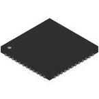
●The ADF7021-N is a high performance, low power, narrow-band transceiver based on the ADF7021. The ADF7021-N has IF filter bandwidths of 9 kHz, 13.5 kHz, and 18.5 kHz, making it ideally suited to worldwide narrowband standards and particularly those that stipulate 12.5 kHz channel separation.
●It is designed to operate in the narrow-band, license-free ISM bands and in the licensed bands with frequency ranges of 80 MHz to 650 MHz and 842 MHz to 916 MHz. The part has both Gaussian and raised cosine transmit data filtering options to improve spectral efficiency for narrow-band applications. It is suitable for circuit applications targeted at the Japanese ARIB STD-T67, the European ETSI EN 300 220, the Korean short range device regulations, the Chinese short range device regulations, and the North American FCC Part 15, Part 90, and Part 95 regulatory standards. A complete transceiver can be built using a small number of external discrete components, making the ADF7021-N very suitable for price-sensitive and area-sensitive applications.
●The range of on-chip FSK modulation and data filtering options allows users greater flexibility in their choice of modulation schemes while meeting the tight spectral efficiency requirements. The ADF7021-N also supports protocols that dynamically switch among 2FSK, 3FSK, and 4FSK to maximize communica-tion range and data throughput.
●The transmit section contains two voltage controlled oscillators (VCOs) and a low noise fractional-N PLL with an output resolution of <1 ppm. The ADF7021-N has a VCO using an internal LC tank (421 MHz to 458 MHz, 842 MHz to 916 MHz) and a VCO using an external inductor as part of its tank circuit (80 MHz to 650 MHz). The dual VCO design allows dual-band operation where the user can transmit and/or receive at any frequency supported by the internal inductor VCO and can also transmit and/or receive at a particular frequency band supported by the external inductor VCO.
●The frequency-agile PLL allows the ADF7021-N to be used in frequency-hopping, spread spectrum (FHSS) systems. Both VCOs operate at twice the fundamental frequency to reduce spurious emissions and frequency pulling problems.
●The transmitter output power is programmable in 63 steps from −16 dBm to +13 dBm and has an automatic power ramp control to prevent spectral splatter and help meet regulatory standards. The transceiver RF frequency, channel spacing, and modulation are programmable using a simple 3-wire interface. The device operates with a power supply range of 2.3 V to 3.6 V and can be powered down when not in use.
●A low IF architecture is used in the receiver (100 kHz), which minimizes power consumption and the external component count yet avoids dc offset and flicker noise at low frequencies. The IF filter has programmable bandwidths of 9 kHz, 13.5 kHz, and 18.5 kHz. The ADF7021-N supports a wide variety of pro-grammable features including Rx linearity, sensitivity, and IF bandwidth, allowing the user to trade off receiver sensitivity and selectivity against current consumption, depending on the application. The receiver also features a patent-pending automatic frequency control (AFC) loop with programmable pull-in range that allows the PLL to track out the frequency error in the incoming signal.
●The receiver achieves an image rejection performance of 56 dB using a patent-pending IR calibration scheme that does not require the use of an external RF source.
●An on-chip ADC provides readback of the integrated tempera-ture sensor, external analog input, battery voltage, and RSSI signal, which provides savings on an ADC in some applications. The temperature sensor is accurate to ±10°C over the full oper-ating temperature range of −40°C to +85°C. This accuracy can be improved by performing a 1-point calibration at room temperature and storing the result in memory.
●### Features and Benefits
● Low power, narrow-band transceiver
● Frequency bands using dual VCO
●80 MHz to 650 MHz
●842 MHz to 916 MHz
● Programmable IF filter bandwidths of
●9 kHz, 13.5 kHz, and 18.5 kHz
● Modulation schemes: 2FSK, 3FSK, 4FSK, MSK
● Spectral shaping: Gaussian and raised cosine filtering
● Fully automatic frequency control loop (AFC)
● On-chip, 7-bit ADC and temperature sensor
● On-chip VCO and fractional-N PLL
● Data rates supported: 0.05 kbps to 24 kbps
● 2.3 V to 3.6 V power supply
● Programmable output power
●−16 dBm to +13 dBm in 63 steps
● Automatic power amplifier (PA) ramp control
● Receiver sensitivity
●−130 dBm at 100 bps, 2FSK
●−122 dBm at 1 kbps, 2FSK
● Patent pending, on-chip image rejection calibration
● Digital received signal strength indication (RSSI)
● Integrated Tx/Rx switch
● 0.1 μA leakage current in power-down mode


