●Product Details
●The ADL5391 draws on three decades of experience in advanced analog multiplier products. It provides the same general mathematical function that has been field proven to provide an exceptional degree of versatility in function synthesis:
●V_W_ = α × (V_X_ x VY)/1 V + V_Z_
●The most significant advance in the ADL5391 is the use of a new multiplier core architecture, which differs markedly from the conventional form that has been in use since 1970. The conventional structure that employs a current mode, translinear core is fundamentally asymmetric with respect to the X and Y inputs, leading to relative amplitude and timing misalignments that are problematic at high frequencies. The new multiplier core eliminates these misalignments by offering symmetric signal paths for both X and Y inputs. The Z input allows a signal to be added directly to the output. This can be used to cancel a carrier or to apply a static offset voltage.
●The fully differential X, Y, and Z input interfaces are operational over a ±2 V range, and they can be used in single-ended fashion. The user can apply a common mode at these inputs to vary from the internally set VPOS/2 down to ground. If these inputs are ac-coupled, their nominal voltage will be VPOS/2. These input interfaces each present a differential 500 Ω input impedance up to approximately 700 MHz, decreasing to 50 Ω at 2 GHz. The gain scaling input, GADJ, can be used for fine adjustment of the gain scaling constant (α) about unity.
●The differential output can swing ±2 V about the VPOS/2 common-mode and can be taken in a single-ended fashion as well. The output common mode is designed to interface directly to the inputs of another ADL5391. Light dc loads can be ground referenced; however, ac-coupling of the outputs is recommended for heavy loads.
●The ENBL pin allows the ADL5391 to be disabled quickly to a standby mode. It operates off supply voltages from 4.5 V to 5.5 V while consuming approximately 130 mA.
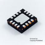
●The ADL5391 is fabricated on Analog Devices, Inc. proprietary, high performance, 65 GHz, SOI complementary, SiGe bipolar IC process. It is available in a 16-lead, RoHS compliant, LFCSP and operates over a −40°C to +85°C temperature range. Evaluation boards are available.
●Applications
● Wideband multiplication and summing
● High frequency analog modulation
● Adaptive antennas (diversity/phased array)
● Square-law detectors and true rms detectors
● Accurate polynomial function synthesis
● DC capable VGA with very fast control
●### Features and Benefits
● Ultrafast symmetric multiplier
● Function: VW = α × (VX × VY)/1 V + VZ
● Unique design ensures absolute XY-symmetry
● Identical X and Y amplitude/timing responses
● Adjustable gain scaling, α
● DC-coupled throughout, 3 dB bandwidth of 2 GHz
● Fully differential inputs, may be used single ended
● Low noise, high linearity
● Accurate, temperature stable gain scaling
● Single-supply operation (4.5 V to 5.5 V at 130 mA)
● Low current power-down mode
● 16-lead LFCSP


