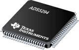
●The ADS5294 is a low-power 80-MSPS 8-Channel ADC that uses CMOS process technology and innovative circuit techniques. Low power consumption, high SNR, low SFDR, and consistent overload recovery allow users to design high-performance systems.
●The digital processing block of the ADS5294 integrates several commonly used digital functions for improving system performance. The device includes a digital filter module that has built-in decimation filters (with lowpass, highpass and bandpass characteristics). The decimation rate is also programmable (by 2, by 4, or by 8). This rate is useful for narrow-band applications, where the filters are used to conveniently improve SNR and knock-off harmonics, while at the same time reducing the output data rate. The device includes an averaging mode where two channels (or even four channels) are averaged to improve SNR.
●Serial LVDS outputs reduce the number of interface lines and enable the highest system integration. The digital data from each channel ADC is output over one or two wires of LVDS output lines depending on the ADC sampling rate. This 2-wire interface maintains a low serial-data rate, allowing low-cost FPGA-based receivers to be used even at a high sample rate. The ADC resolution is programmed to 12-bit or 14-bit through registers. A unique feature is the programmable-mapping module that allows flexible mapping between the input channels and the LVDS output pins. This module greatly reduces the complexity of LVDS-output routing, and by reducing the number of PCB layers, potentially results in cheaper system boards.
●The device integrates an internal reference trimmed to accurately match across devices. Internal reference mode achieves the best performance. External references can also drive the device.
●The device is available in a 12-mm × 12-mm 80-pin QFP package. The device is specified over a 40°C to 85°C operating temperature range. ADS5294 is completely pin-to-pin and register compatible to ADS5292.


