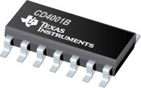
●CD4001B, CD4002B, and CD4025B NOR gates provide the system designer with direct implementation of the NOR function and supplement the existing family of CMOS gates. All inputs and outputs are buffered.
●The CD4001B, CD4002B, and CD4025B types are supplied in 14-lead hermetic dual-in-line ceramic packages (F3A suffix), 14-lead dual-in-line plastic packages (E suffix), 14-lead small-outline packages (M, MT, M96, and NSR suffixes), and 14-lead thin shrink small-outline packages (PW and PWR suffixes).
● Propagation delay time = 60 ns (typ.) at CL = 50 pF, VDD = 10 V
● Buffered inputs and outputs
● Standardized symmetrical output characteristics
● 100% tested for maximum quiescent current at 20 V
● 5-V, 10-V, and 15-V parametric ratings
● Maximum input current of 1 µA at 18 V over full package-temperature range; 100 nA at 18 V and 25°C
● Noise margin (over full package temperature range):
● 1 V at VDD = 5 V
● 2 V at VDD = 10 V
● 2.5 V at VDD = 15 V
● Meets all requirements of JEDEC Tentative Standard No. 13B, "Standard Specifications for Description of B Series CMOS Devices"
●Data sheet acquired from Harris Semiconductor


