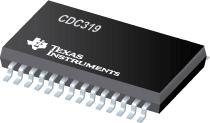
●The CDC319 is a high-performance clock buffer that distributes one input (A) to 10 outputs (Y) with minimum skew for clock distribution. The CDC319 operates from a 3.3-V power supply, and is characterized for operation from 0°C to 70°C.
●The device provides a standard mode (100K-bits/s) I2C serial interface for device control. The implementation is as a slave/receiver. The device address is specified in the I2C device address table. Both of the I2C inputs (SDATA and SCLOCK) provide integrated pullup resistors (typically 140 k) and are 5-V tolerant.
●Three 8-bit I2C registers provide individual enable control for each of the outputs. All outputs default to enabled at powerup. Each output can be placed in a disabled mode with a low-level output when a low-level control bit is written to the control register. The registers are write only and must be accessed in sequential order (i.e., random access of the registers is not supported).
●The CDC319 provides 3-state outputs for testing and debugging purposes. The outputs can be placed in a high-impedance state via the output-enable (OE) input. When OE is high, all outputs are in the operational state. When OE is low, the outputs are placed in a high-impedance state. OE provides an integrated pullup resistor.
● High-Speed, Low-Skew 1-to-10 Clock Buffer for SDRAM (Synchronous DRAM) Clock Buffering Applications
● Output Skew, tsk(o), Less Than 250 ps
● Pulse Skew, tsk(p), Less Than 500 ps
● Supports up to Two Unbuffered SDRAM DIMMs (Dual Inline Memory Modules)
● I2C Serial Interface Provides Individual Enable Control for Each Output
● Operates at 3.3 V
● Distributed VCC and Ground Pins Reduce Switching Noise
● ESD Protection Exceeds 2000 V Per MIL-STD-883, Method 3015
● Packaged in 28-Pin Shrink Small Outline (DB) Package


