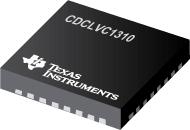
●The CDCLVC1310 is a highly versatile, low-jitter, low-power clock fanout buffer which can distribute to ten low-jitter LVCMOS clock outputs from one of three inputs, whose primary and secondary inputs can feature differential or single-ended signals and crystal input. Such a buffer is good for use in a variety of mobile and wired infrastructure, data communication, computing, low-power medical imaging, and portable test and measurement applications. When the input is an illegal level, the output is at a defined state. One can set the core to 2.5 V or 3.3 V, and output to 1.5 V, 1.8 V, 2.5 V or 3.3 V. Pin programming easily configures the CDCLVC1310. The overall additive jitter performance is 25 fsRMS (typical). The CDCLVC1310 comes in a small 32-pin 5-mm × 5-mm QFN package.
● High-Performance Crystal Buffer With Ultralow Noise
●Floor of –169 dBc/Hz
● Additive Phase Noise/Jitter Performance Is
●25 fsRMS (Typ.)
● Level Translation With 3.3-V or 2.5-V Core and
●3.3-V, 2.5-V, 1.8-V, or 1.5-V Output Supply
● Device inputs consist of primary, secondary,
●and crystal inputs, and manually selectable
●(through pins) using the input MUX. The primary
●and secondary inputs can accept LVPECL, LVDS,
●HCSL, SSTL or LVCMOS signals and crystal input.
● Crystal Frequencies Supported Are From
●8 MHz to 50 MHz
● Differential and Single-Ended Input Frequencies
●Supported Are up to 200 MHz
● 10 Single-Ended LVCMOS Outputs. The outputs can
●operate at 1.5-V, 1.8-V, 2.5-V or 3.3-V
●Power-Supply Voltage.
● LVCMOS Outputs Operate up to 200 MHz
● Output Skew Is 30 ps (Typical)
● Total Propagation Delay Is 2 ns (Typical)
● Synchronous and Glitch-Free Output Enable Is
●Available
● Offered in QFN-32 5-mm × 5-mm Package With
●Industrial Temperature Range of –40°C to 85°C
● Can Overdrive Crystal Input With LVCMOS Signal up to 50 MHz


