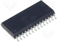
●The DAC811 is a complete, single-chip integrated-circuit, microprocessor-compatible, 12-bit digital-to-analog converter. The chip combines a precision voltage reference, microcomputer interface logic, and double-buffered latch, in a 12-bit D/A converter with a voltage output amplifier. Fast current switches and a laser-trimmed thin-film resistor network provide a highly accurate and fast D/A converter.
●Microcomputer interfacing is facilitated by a double-buffered latch. The input latch is divided into three 4-bit nibbles to permit interfacing to 4-, 8-, 12-, or 16-bit buses and to handle right-or left-justified data. The 12-bit data in the input latches is transferred to the D/A latch to hold the output value.
●Input gating logic is designed so that loading the last nibble or byte of data can be accomplished simultaneously with the transfer of data (previously stored in adjacent latches) from adjacent input latches to the D/A latch. This feature avoids spurious analog output values while using an interface technique that saves computer instructions.
●The DAC811 is laser trimmed at the wafer level and is specified to ±1/4LSB maximum linearity error (B, K, and S grades) at 25°C and °1/2LSB maximum over the temperature range. All grades are guaranteed monotonic over the specification temperature range.
●The DAC811 is available in six performance grades and three package types. DAC811J and K are specified over the temperature ranges of 0°C to +70°C; DAC811A and B are specified over 25°C to +85°C; DAC811R and S are specified over 55°C to +125°C. DAC811J and K are packaged in a reliable 28-pin plastic DIP or plastic SO package, while DAC811A and B are available in a 28-pin 0.6" wide dual-inline hermetically sealed ceramic side-brazed package (H package).

 Part 3D Model
