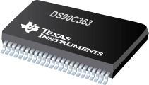
●The DS90C363 transmitter converts 21 bits of CMOS/TTL data into three LVDS (Low Voltage Differential Signaling) data streams. A phase-locked transmit clock is transmitted in parallel with the data streams over a fourth LVDS link. Every cycle of the transmit clock 21 bits of input data are sampled and transmitted. The DS90CF364 receiver converts the LVDS data streams back into 21 bits of CMOS/TTL data. At a transmit clock frequency of 65 MHz, 18 bits of RGB data and 3 bits of LCD timing and control data (FPLINE, FPFRAME, DRDY) are transmitted at a rate of 455 Mbps per LVDS data channel. Using a 65 MHz clock, the data throughput is 170 Mbyte/sec. The Transmitter is offered with programmable edge data strobes for convenient interface with a variety of graphics controllers. The Transmitter can be programmed for Rising edge strobe or Falling edge strobe through a dedicated pin. A Rising edge Transmitter will inter-operate with a Falling edge Receiver (DS90CF364) without any translation logic.
●This chipset is an ideal means to solve EMI and cable size problems associated with wide, high speed TTL interfaces.
● 20 to 65 MHz shift clock support
● Programmable Transmitter (DS90C363) strobe select (Rising or Falling edge strobe)
● Single 3.3V supply
● Chipset (TX + RX) power consumption < 250 mW (typ)
● Power-down mode (< 0.5 mW total)
● Single pixel per clock XGA (1024×768) ready
● Supports VGA, SVGA, XGA and higher addressability
● Up to 170 Megabyte/sec bandwidth
● Up to 1.3 Gbps throughput
● Narrow bus reduces cable size and cost
● 290 mV swing LVDS devices for low EMI
● PLL requires no external components
● Low profile 48-lead TSSOP package
● Falling edge data strobe Receiver
● Compatible with TIA/EIA-644 LVDS standard
● ESD rating > 7 kV
● Operating Temperature: −40°C to +85°C
●All trademarks are the property of their respective owners. TRI-STATE is a trademark of Texas Instruments. TRI-STATE is a trademark of Texas Instruments.


