●DESCRIPTION
●The DS90CR285 transmitter converts 28 bits of LVCMOS/LVTTL data into four LVDS (Low Voltage Differential Signaling) data streams. A phase-locked transmit clock is transmitted in parallel with the data streams over a fifth LVDS link. Every cycle of the transmit clock 28 bits of input data are sampled and transmitted. The DS90CR286 receiver converts the LVDS data streams back into 28 bits of LVCMOS/LVTTL data. At a transmit clock frequency of 66 MHz, 28 bits of TTL data are transmitted at a rate of 462 Mbps per LVDS data channel. Using a 66 MHz clock, the data throughput is 1.848 Gbit/s (231 Mbytes/s).
●The multiplexing of the data lines provides a substantial cable reduction. Long distance parallel single-ended buses typically require a ground wire per active signal (and have very limited noise rejection capability). Thus, for a 28-bit wide data and one clock, up to 58 conductors are required. With the Channel Link chipset as few as 11 conductors (4 data pairs, 1 clock pair and a minimum of one ground) are needed. This provides a 80% reduction in required cable width, which provides a system cost savings, reduces connector physical size and cost, and reduces shielding requirements due to the cables" smaller form factor.
●FEATURES
●• Single +3.3V Supply
●• Chipset (Tx + Rx) Power Consumption <250 mW (typ)
●• Power-Down Mode (<0.5 mW total)
●• Up to 231 Megabytes/sec Bandwidth
●• Up to 1.848 Gbps Data Throughput
●• Narrow Bus Reduces Cable Size
●• 290 mV Swing LVDS Devices for Low EMI
●• +1V Common Mode Range (Around +1.2V)
●• PLL Requires no External Components
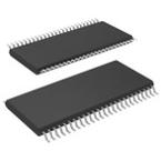
●• Both Devices are Offered in a Low Profile 56-Lead TSSOP Package
●• Rising Edge Data Strobe
●• Compatible with TIA/EIA-644 LVDS Standard
●• ESD Rating > 7 kV
●• Operating Temperature: −40°C to +85°C

 Part 3D Model
