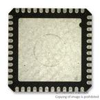
●Product Details
●The HMCAD1520 is a versatile high performance low power analog-to-digital converter (ADC), with interleaving High Speed Modes to increase sampling rate. Integrated Cross Point Switches activate the input selected by the user.
●In Single Channel Mode, one of the four inputs can be selected as valid input to the single ADC channel. In Dual Channel Mode, any two of the four inputs can be selected to each ADC channel. In Quad Channel Mode and Precision Mode, any input can be assigned to any ADC channel. An internal, low jitter and programmable clock divider makes it possible to use a single clock source for all operational modes.
●The HMCAD1520 is based on a proprietary structure, and employs internal reference circuitry, a serial control interface and a serial LVDS output data. Data and frame synchronization clocks are supplied for data capture at the receiver. Internal digital fine gain can be set separately for each ADC to calibrate for gain errors.
●Various modes and configuration settings can be applied to the ADC through the serial control interface (SPI). each channel can be powered down independently and output data format can be selected through this interface. A full chip idle mode can be set by a single external pin.
●Register settings determine the exact function of this pin. HMCAD1520 is designed to interface easily with Field Programmable Gate Arrays (FPGAs) from several vendors.
●Applications
● Precision Oscilloscopes
● Spectrum Analyzers
● Diversity Receivers
● Hi-End Ultrasound
● Communication Testing
● Non Destructive Testing
●### Features and Benefits
● High Speed Modes (12-bit / 8-bit)
●Quad Channel Mode: FSmax = 160 / 250 MSPS
●Dual Channel Mode: FSmax = 320 / 500 MSPS
●Single Channel Mode: FSmax = 640 / 1000 MSPS
●SNR: 70 dB, SFDR: 60/75 dB
●(12-bit 1ch Mode)
● 8-bit Modes Described in HMCAD1511 and HMCAD1510
● Precision Mode (14-bit)
●Four channels up to 105 MSPS
●SNR : 74 dB, SFDR: 83 dB @ 70 MHz
●SNR : 72.5 dB, SFDR: 78 dB @ 140 MHz
● Integrated Cross Point Switches with instantaneous switching
● Internal low jitter programmable Clock Divider
● Ultra Low Power Dissipation
●490 mW including I/O at 12-bit 640 MSPS
● 0.5 μs start-up time from Sleep,
●15 μs from Power Down
● Internal reference circuitry with no external components required
● Coarse and fine gain control
● Digital fine gain adjustment for each ADC
● Internal offset correction
● 1.8 V supply voltage
● 1.7 - 3.6 V CMOS logic on control interface pins
● Serial LVDS output
●12, 14, 16 and Dual 8-bit modes available
● 7 x 7 mm 48 QFN Package


