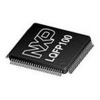
●Overview
●The LPC11U6x family builds on the ease-of-use and design flexibility of NXP’s award-winning LPC11Uxx portfolio with a range of enhanced features, including a more energy-efficient ARM® Cortex™-M0+ core, significantly more flash and SRAM, more serial communications, a new 2-Msps ADC and more versatile timers. These additional features allow the LPC11U6x to tackle a wider range of applications in consumer, commercial and industrial markets such as metering and data collection, wired and wireless routing, handheld medical equipment, and PC/gaming accessories, among others.
●The LPC11U6x family includes a USB device controller certified by the USB Implementers Forum (USB-IF) and gives designers access to all the USB software, tools and shortcuts they need to simplify development and shrink time to market. Embedding the USB drivers in ROM cuts design time and reduces application program footprint while increasing reliability; and an on-chip PHY reduces the solution BOM and design complexity.
●To support more demanding data and buffering requirements, as well as larger application code sizes, the LPC11U6x extends memory options by doubling flash to 256 KB and tripling SRAM to 36 KB. More rigorous I/O requirements are supported by expanded serial connectivity, including 5 USARTs, 2 I²Cs, 2 SPIs, and up to 80 GPIOs, along with a new 12-channel, 12-bit, 2-Msps ADC for higher bandwidth and higher-precision input.
●LPC11U6x also include both standard and configurable timers/PWMs for advanced timing requirements. Higher operating temperatures (up to 105 ºC) make them suitable for more commercial and industrial environments.
●Samples are currently available for ordering through Digi-Key and Mouser.
●MoreLess
●## Features
●### System
● ARM Cortex-M0+ processor, running at frequencies of up to 50 MHz with single-cycle multiplier and fast single-cycle I/O port.
● ARM Cortex-M0+ built-in Nested Vectored Interrupt Controller (NVIC).
● AHB Multilayer matrix.
● System tick timer.
● Serial Wire Debug (SWD) and JTAG boundary scan modes supported.
● Micro Trace Buffer (MTB) supported.
●### Memory
● Up to 256 kB on-chip flash programming memory with page erase.
● Up to 36 kB main SRAM.
● Up to two additional SRAM blocks of 2 kB each.
● Up to 4 kB EEPROM.
●### ROM API support
● Boot loader.
● USART drivers.
● I²C drivers.
● USB drivers.
● DMA drivers.
● Power profiles.
● Flash In-Application Programming (IAP) and In-System Programming (ISP).
● 32-bit integer division routines.
●### Digital peripherals
● Simple DMA engine with 16 channels and programmable input triggers.
● High-speed GPIO interface connected to the ARM Cortex-M0+ IO bus with up to 80 General-Purpose I/O (GPIO) pins with configurable pull-up/pull-down resistors, programmable open-drain mode, input inverter, and programmable glitch filter and digital filter.
● Pin interrupt and pattern match engine using eight selectable GPIO pins.
● Two GPIO group interrupt generators.
● CRC engine.
●### Configurable PWM/timer subsystem
● Up to four 32-bit and two 16-bit counter/timers or two 32-bit and four 16-bit counter/timers.
● Up to 21 match outputs and 16 capture inputs.
● Up to 19 PWM outputs with 6 independent time bases.
● Two State-Configurable Timers (SCTimer/PWM) for highly flexible, event-driven timing and PWM applications.
● Two 16-bit and two 32-bit standard counter/timers.
●### Analog peripherals
● One 12-bit ADC with up to 12 input channels with multiple internal and external trigger inputs and with sample rates of up to 2 Msamples/s. The ADC supports two independent conversion sequences.
● Temperature sensor.
●### Serial interfaces
● Up to five USART interfaces, all with DMA, synchronous mode, and RS-485 mode support. Four USARTs use a shared fractional baud generator.
● Two SSP controllers with DMA support.
● Two I²C-bus interfaces. One I²C-bus interface with specialized open-drain pins supports I²C Fast-mode plus.
● USB 2.0 full-speed device controller with on-chip PHY. XTAL-less low-speed mode supported.
●### Clock generation
● 12 MHz internal RC oscillator trimmed to 1 % accuracy that can optionally be used as a system clock.
● On-chip 32 kHz oscillator for RTC.
● Crystal oscillator with an operating range of 1 MHz to 25 MHz. Oscillator pins are shared with the GPIO pins.
● Programmable watchdog oscillator with a frequency range of 9.4 kHz to 2.3 MHz.
● PLL allows CPU operation up to the maximum CPU rate without the need for a high-frequency crystal.
● A second, dedicated PLL is provided for USB.
● Clock output function with divider that can reflect the crystal oscillator, the main clock, the IRC, or the watchdog oscillator.
●### Power control
● Integrated PMU (Power Management Unit) to minimize power consumption.
● Reduced power modes: Sleep mode, Deep-sleep mode, Power-down mode, and Deep power-down mode.
● Wake-up from Deep-sleep and Power-down modes on external pin inputs and USART activity.
● Power-On Reset (POR).
● Brownout detect.
●### Additional Features
● Windowed Watchdog timer (WWDT).
● Real-time Clock (RTC) in the always-on power domain with separate battery supply pin and 32 kHz oscillator.
● Unique device serial number for identification.
● Single power supply (2.4 V to 3.6 V).
● Separate VBAT supply for RTC.
● Operating temperature range -40 °C to 105 °C.
● Available as LQFP100 package
●## Target Applications
● Three-phase e-meter
● GPS tracker
● Gaming accessories
● Car radio
● Medical monitor
● PC peripherals

 Part 3D Model
