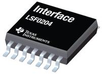
●The LSF family consists of bidirectional voltage level translators that operate from 0.8 V to 4.5 V (Vref_A) and 1.8 V to 5.5 V (Vref_B). This range allows for bidirectional voltage translations between 0.8 V and 5.0 V without the need for a direction terminal in open-drain or push-pull applications. The LSF family supports level translation applications with transmission speeds greater than 100 MHz for open-drain systems that utilize a 15-pF capacitance and 165-Ω pull-up resistor.
●When the An or Bn port is LOW, the switch is in the ON-state and a low resistance connection exists between the An and Bn ports. The low Ron of the switch allows connections to be made with minimal propagation delay and signal distortion. The voltage on the A or B side will be limited to Vref_A and can be pulled up to any level between Vref_A and 5 V. This functionality allows a seamless translation between higher and lower voltages selected by the user without the need for directional control.
●The supply voltage (Vpu#) for each channel may be individually set up with a pull up resistor. For example, CH1 may be used in up-translation mode (1.2 V ↔ 3.3 V) and CH2 in down-translation mode (2.5 V ↔ 1.8 V).
●When EN is HIGH, the translator switch is on, and the An I/O is connected to the Bn I/O, respectively, allowing bidirectional data flow between ports. When EN is LOW, the translator switch is off, and a high-impedance state exists between ports. The EN input circuit is designed to be supplied by Vref_A. EN must be LOW to ensure the high-impedance state during power-up or power-down.
● Provides Bidirectional Voltage Translation With No
●Direction Terminal
● Supports up to 100-MHz up Translation and
●Greater Than 100-MHz Down Translation
●at ≤ 30-pF Capacitor Load and up to 40-MHz
●Up/Down Translation at 50-pF Capacitor Load
● Supports Ioff, Partial Power Down Mode (Refer to
●_Feature Description_)
● Allows Bidirectional Voltage Level Translation
●Between
● 0.8 V ↔ 1.8, 2.5, 3.3, 5 V
● 1.2 V ↔ 1.8, 2.5, 3.3, 5 V
● 1.8 V ↔ 2.5, 3.3, 5 V
● 2.5 V ↔ 3.3, 5 V
● 3.3 V ↔ 5 V
● Low Standby Current
● 5 V Tolerance I/O Port to Support TTL
● Low Ron Provides Less Signal Distortion
● High-Impedance I/O Terminals For EN = Low
● Flow-Through Pinout for Ease PCB Trace Routing
● Latch-Up Performance Exceeds 100 mA Per
●JESD17
● –40°C to 125°C Operating Temperature Range
● ESD Performance Tested Per JESD 22
● 2000-V Human-Body Model (A114-B, Class II)
● 200-V Machine Model (A115-A)
● 1000-V Charged-Device Model (C101)


