●Overview
●The PCA9510A is a hot swappable I²C-bus and SMBus buffer that allows I/O card insertion into a live backplane without corrupting the data and clock buses. Control circuitry prevents the backplane from being connected to the card until a stop command or bus idle occurs on the backplane without bus contention on the card. When the connection is made, the PCA9510A provides bidirectional buffering, keeping the backplane and card capacitances isolated.
●The PCA9510A has no rise time accelerator circuitry to prevent interference when there are multiple devices in the same system. The PCA9510A incorporates a digital ENABLE input pin, which enables the device when asserted HIGH and forces the device into a Low current mode when asserted LOW, and an open-drain READY output pin, which indicates that the backplane and card sides are connected together (HIGH) or not (LOW).
●During insertion, the PCA9510A SDAIN and SCLIN pins (inputs only) are precharged to 1 V to minimize the current required to charge the parasitic capacitance of the chip.
●Remark
●: The dynamic offset design of the PCA9510A/11A/12A/13A/14A I/O drivers allow them to be connected to another PCA9510A/11A/12A/13A/14A device in series or in parallel and to the A side of the PCA9517. The PCA9510A/11A/12A/13A/14A
●cannot
●connect to the static offset I/Os used on the PCA9515/15A/16/16A/18 or PCA9517 B side or P82B96 Sx/y side.
●MoreLess
●## Features
● Bidirectional buffer for SDA and SCL lines increases fan-out and prevents SDA and SCL corruption during live board insertion and removal from multipoint backplane systems
● Compatible with Standard-mode I²C-bus, Fast-mode I²C-bus, and SMBus standards
● Active HIGH ENABLE input
● Active HIGH READY open-drain output
● High-impedance SDAn and SCLn pins for VCC = 0 V
● 1 V precharge on SDAIN and SCLIN inputs
● Supports clock stretching and multiple master arbitration and synchronization
● Operating power supply voltage range: 2.7 V to 5.5 V
● 5 V tolerant I/Os
● 0 Hz to 400 kHz clock frequency
● ESD protection exceeds 2000 V HBM per JESD22-A114, 200 V MM per JESD22-A115, and 1000 V CDM per JESD22-C101
● Latch-up testing is done to JEDEC Standard JESD78 which exceeds 100 mA
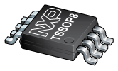
● Packages offered: SO8, TSSOP8 (MSOP8)
●## Target Applications
● cPCI, VME, AdvancedTCA cards and other multipoint backplane cards that are required to be inserted or removed from an operating system
●## Features

 Part 3D Model
