●DEVICE OVERVIEW
●This document contains device specific information for the following devices:
●• PIC18F248
●• PIC18F258
●• PIC18F448
●• PIC18F458
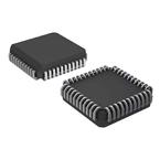
●These devices are available in 28-pin, 40-pin and 44-pin packages. They are differentiated from each other in four ways:
●1\. PIC18FX58 devices have twice the Flash program memory and data RAM of PIC18FX48 devices (32 Kbytes and 1536 bytes vs. 16 Kbytes and 768 bytes, respectively).
●2\. PIC18F2X8 devices implement 5 A/D channels, as opposed to 8 for PIC18F4X8 devices.
●3\. PIC18F2X8 devices implement 3 I/O ports, while PIC18F4X8 devices implement 5.
●4\. Only PIC18F4X8 devices implement the Enhanced CCP module, analog comparators and the Parallel Slave Port.
●All other features for devices in the PIC18FXX8 family, including the serial communications modules, are identical. These are summarized in Table 1-1. Block diagrams of the PIC18F2X8 and PIC18F4X8 devices are provided in Figure 1-1 and Figure 1-2, respectively. The pinouts for these device families are listed in Table 1-2.
●High-Performance RISC CPU:
●• Linear program memory addressing up to 2 Mbytes
●• Linear data memory addressing to 4 Kbytes
●• Up to 10 MIPS operation
●• DC – 40 MHz clock input
●• 4 MHz-10 MHz oscillator/clock input with PLL active
●• 16-bit wide instructions, 8-bit wide data path
●• Priority levels for interrupts
●• 8 x 8 Single-Cycle Hardware Multiplier
●Peripheral Features:
●• High current sink/source 25 mA/25 mA
●• Three external interrupt pins
●• Timer0 module: 8-bit/16-bit timer/counter with 8-bit programmable prescaler
●• Timer1 module: 16-bit timer/counter
●• Timer2 module: 8-bit timer/counter with 8-bit period register (time base for PWM)
●• Timer3 module: 16-bit timer/counter
●• Secondary oscillator clock option – Timer1/Timer3
●• Capture/Compare/PWM (CCP) modules; CCP pins can be configured as:
●\- Capture input: 16-bit, max resolution 6.25 ns
●\- Compare: 16-bit, max resolution 100 ns (TCY)
●\- PWM output: PWM resolution is 1 to 10-bit
● Max. PWM freq. @:8-bit resolution = 156 kHz
● 10-bit resolution = 39 kHz
●• Enhanced CCP module which has all the features of the standard CCP module, but also has the following features for advanced motor control:
●\- 1, 2 or 4 PWM outputs
●\- Selectable PWM polarity
●\- Programmable PWM dead time
●• Master Synchronous Serial Port (MSSP) with two modes of operation:
●\- 3-wire SPI™ (Supports all 4 SPI modes)
●\- I2C™ Master and Slave mode
●• Addressable USART module:
●\- Supports interrupt-on-address bit
●Advanced Analog Features:
●• 10-bit, up to 8-channel Analog-to-Digital Converter module (A/D) with:
●\- Conversion available during Sleep
●\- Up to 8 channels available
●• Analog Comparator module:
●\- Programmable input and output multiplexing
●• Comparator Voltage Reference module
●• Programmable Low-Voltage Detection (LVD) module:
●\- Supports interrupt-on-Low-Voltage Detection
●• Programmable Brown-out Reset (BOR) CAN bus Module Features:
●• Complies with ISO CAN Conformance Test
●• Message bit rates up to 1 Mbps
●• Conforms to CAN 2.0B Active Spec with:
●\- 29-bit Identifier Fields
●\- 8-byte message length
●\- 3 Transmit Message Buffers with prioritization
●\- 2 Receive Message Buffers
●\- 6 full, 29-bit Acceptance Filters
●\- Prioritization of Acceptance Filters
●\- Multiple Receive Buffers for High Priority
● Messages to prevent loss due to overflow
●\- Advanced Error Management Features
●Special Microcontroller Features:
●• Power-on Reset (POR), Power-up Timer (PWRT) and Oscillator Start-up Timer (OST)
●• Watchdog Timer (WDT) with its own on-chip RC oscillator
●• Programmable code protection
●• Power-saving Sleep mode
●• Selectable oscillator options, including:
●\- 4x Phase Lock Loop (PLL) of primary oscillator
●\- Secondary Oscillator (32 kHz) clock input
●• In-Circuit Serial ProgrammingTM (ICSPTM) via two pins
●Flash Technology:
●• Low-power, high-speed Enhanced Flash technology
●• Fully static design
●• Wide operating voltage range (2.0V to 5.5V)
●• Industrial and Extended temperature ranges

 Part 3D Model
