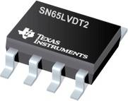
●The SN65LVDS1, SN65LVDS2, and SN65LVDT2 devices are single, low-voltage, differential line drivers and receivers in the small-outline transistor package. The outputs comply with the TIA/EIA-644 standard and provide a minimum differential output voltage magnitude of 247 mV into a 100-Ω load at signaling rates up to 630 Mbps for drivers and 400 Mbps for receivers.
●When the SN65LVDS1 device is used with an LVDS receiver (such as the SN65LVDT2) in a point-to-point connection, data or clocking signals can be transmitted over printed-circuit board traces or cables at very high rates with very low electromagnetic emissions and power consumption. The packaging, low power, low EMI, high ESD tolerance, and wide supply voltage range make the device ideal for battery-powered applications.
●The SN65LVDS1, SN65LVDS2, and SN65LVDT2 devices are characterized for operation from –40°C to 85°C.
● Meets or Exceeds the ANSI TIA/EIA-644 Standard
● Designed for Signaling Rates1 up to:
● 630 Mbps for Drivers
● 400 Mbps for Receivers
● Operates From a 2.4-V to 3.6-V Supply
● Available in SOT-23 and SOIC Packages
● Bus-Terminal ESD Exceeds 9 kV
● Low-Voltage Differential Signaling With Typical Output
●Voltages of 350 mV Into a 100-Ω Load
● Propagation Delay Times
● 1.7-ns Typical Driver
● 2.5-ns Typical Receiver
● Power Dissipation at 200 MHz
● 25 mW Typical Driver
● 60 mW Typical Receiver
● LVDT Receiver Includes Line Termination
● Low Voltage TTL (LVTTL) Level Driver Input Is 5-V
●Tolerant
● Driver Is Output High-Impedance with VCC < 1.5 V
● Receiver Output and Inputs are High-Impedance With
●VCC < 1.5 V
● Receiver Open-Circuit Fail Safe
● Differential Input Voltage Threshold Less Than 100 mV


