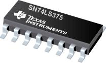
●The SN54LS375 and SN74LS375 bistable latches are electrically and functionally identical to the SN54LS75 and SN74LS75, respectively. Only the arrangement of the terminals has been changed in the SN54LS375 and SN74LS375.
●These latches are ideally suited for use as temporary storage for binary information between processing units and input/output or indicator units. Information present at a data (D) input is transferred to the Q output when the enable (C) is high and the Q output will follow the data input as long as the enable remains high. When the enable goes low, the information (that was present at the data input at the time the transition occurred) is retained at the Q output until the enable goes high.
●All inputs are diode-clamped to minimize transmission-line effects and simplify system design. The SN54LS375 is characterized for operation over the full military temperature range of -55°C to 125°C; SN74LS375 is characterized for operation from 0°C to 70°C.
● Supply Voltage and Ground on Corner Pins To Simplify P-C Board Layout
TI
Buffer/Line Driver 1CH Non-Inverting 3-ST CMOS 5Pin SC-70 T/R
TI
Buffer/Line Driver 1CH Non-Inverting 3-ST CMOS 5Pin SOT-23 T/R
TI
Shift Register, HC Family, 74HC164, Serial to Parallel, 1Element, 8Bit, DIP, 14Pins
TI
Inverter, Schmitt Trigger, 74LVC1G14, 1Input, 32mA, 1.65V to 5.5V, SOT-23-5
TI
Inverter Schmitt Trigger 6Element CMOS 14Pin TSSOP Inverter Schmitt Trigger 6Element CMOS 14Pin TSSOP
TI
Buffer/Line Driver 8CH Non-Inverting 3-ST CMOS 20Pin TSSOP T/R
TI
Inverter, Schmitt Trigger, 74AHC1G14, 1Input, 8mA, 2V to 5.5V, SOT-23-5
TI
TEXAS INSTRUMENTS SN74LVC4245APWR Transceiver, Non-Inverting, 2.7V to 3.6V, 4.5V to 5.5V, TSSOP-24
TI
OR Gate 1Element 2IN CMOS 5Pin SOT-23 T/R
TI
Flip-Flop, Differential / Complementary, Positive Edge, 74LVC74, D, 4.1ns, 200MHz, 32mA, VSSOP
Part Datasheet PDF Search
72,405,303 Parts Datasheet PDF, Update more than 5,000 PDF files ervery day.


