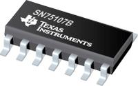
●These circuits are TTL-compatible, high-speed line receivers. Each is a monolithic dual circuit featuring two independent channels. They are designed for general use, as well as for such specific applications as data comparators and balanced, unbalanced, and party-line transmission systems. These devices are unilaterally interchangeable with and are replacements for the SN55107, SN75107, and SN75108, but offer diode-clamped strobe inputs to simplify circuit design.
●The essential difference between the A and B versions can be seen in the schematics. Input-protection diodes are in series with the collectors of the differential-input transistors of the B versions. These diodes are useful in certain party-line systems that have multiple VCC+ power supplies and can be operated with some of the VCC+ supplies turned off. In such a system, if a supply is turned off and allowed to go to ground, the equivalent input circuit connected to that supply would be as follows:
●This would be a problem in specific systems that might have the transmission lines biased to some potential greater than 1.4 V.
●The SN55107A is characterized for operation over the full military temperature range of -55°C to 125°C. The SN75107A, SN75107B, and SN75108A are characterized for operation from 0°C to 70°C.
●H = high level, L = low level, X = irrelevant
● High Speed
● Standard Supply Voltage
● Dual Channels
● High Common-Mode Rejection Ratio
● High Input Impedance
● High Input Sensitivity
● Differential Common-Mode Input Voltage Range of ±3 V
● Strobe Inputs for Receiver Selection
● Gate Inputs for Logic Versatility
● TTL Drive Capability
● High dc Noise Margin
● Totem-Pole Outputs
● B Version Has Diode-Protected Input for Power-Off Condition


