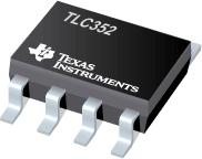
●This device is fabricated using LinCMOS technology and consists of two independent voltage comparators, each designed to operate from a single power supply. Operation from dual supplies is also possible if the difference between the two supplies is 1.4 V to 18 V. Each device features extremely high input impedance (typically greater than 1012 ), which allows direct interface to high-impedance sources. The output are n-channel open-drain configurations and can be connected to achieve positive-logic wired-AND relationships. The capability of the TLC352 to operate from 1.4-V supply makes this device ideal for low-voltage battery applications.
●The TLC352 has internal electrostatic discharge (ESD) protection circuits and has been classified with a 2000-V ESD rating tested under MIL-STD-883C, Method 3015. However, care should be exercised in handling this device as exposure to ESD may result in degradation of the device parametric performance.
●The TLC352C is characterized for operation from 0°C to 70°C. The TLC352I is characterized for operation over the industrial temperature range of 40°C to 85°C.
● Single- or Dual-Supply Operation
● Wide Range of Supply Voltages
● 1.5 V to 18 V
● Very Low Supply Current Drain
● 150 uA Typ at 5 V
● 65 uA Typ at 1.4 V
● Built-In ESD Protection
● High Input Impedance ...1012 Typ
● Extremely Low Input Bias Current 5 pA Typ
● Ultrastable Low Input Offset Voltage
● Input Offset Voltage Change at Worst-Case Input Conditions Typically 0.23 uV/ Month, Including the First 30 Days
● Common-Mode Input Voltage Range Includes Ground
● Outputs Compatible With TTL, MOS, and CMOS
● Pin-Compatible With LM393
●LinCMOS is a trademark of Texas Instruments Incorporated.

 Part 3D Model
