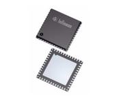
●Description:
●The TLE9877QXA20 family is part of the TLE987x product family. The TLE9877QXA20 is a single chip 3-Phase motor driver that integrates the industry standard ARM® Cortex™ M3 core, enabling the implementation of advanced motor control algorithms such as field-oriented control. It includes six fully integrated NFET drivers optimized to drive a 3-Phase motor via six external power NFETs, a charge pump enabling low voltage operation and programmable current along with current slope control for optimized EMC behavior. Its peripheral set includes a current sensor, a successive approximation ADC synchronized with the capture and compare unit for PWM control and 16-bit timers. A LIN transceiver is also integrated to enable communication to the device along with a number of general purpose I/Os. It includes an on-chip linear voltage regulator to supply external loads. It includes an on-chip linear voltage regulator to supply external loads.
●It is a highly integrated automotive qualified device enabling cost and space efficient solutions for mechatronic BLDC motor drive applications such as pumps and fans.
●Summary of Features:
● Six current programmable Drivers with charge pump for N-Channel MOSFET
● Integrated LIN transceiver compatible with LIN 2.2 and SAEJ2602
● Two Full duplex serial interface (UART) with LIN support
● Two Synchronous serial channel (SSC)
● On-chip OSC and PLL for clock generation
● One high voltage monitoring input with wake up functionality
● High speed Operational amplifier for motor current sensing via shunt
● Measurement unit:
● 8-bit ADC module with 10 multiplexed inputs
● 10-bit ADC module with 8 multiplexed inputs, 5 external Analog inputs
● On chip temperature and battery voltage measurement unit
● Independent Programmable window watchdog
● 5V/1.5V Internal supplies
● External Supply (VDDEXT): 5V+/-2% @ 20mA
● Power saving modes:
● MCU slow-down Mode
● Sleep Mode
● Stop Mode
● Cyclic wake-up Sleep Mode
●## Features of the Microcontroller:
● 32 bit ARM Cortex M3 Core, up to 24 MHz clock frequency
● 64 kByte flash memory for code and data
● 32 kByte Boot ROM memory in code space (used for boot code and IP storage)
● 6 kByte RAM memory
● Harvard architecture
● Thumb®-2 Instruction Set and hardware divide and multiplication unit
● Four 16-Bit timers
● Capture/compare unit for PWM signal generation (CCU6) with 2 x 16-bits timers
●## General Characteristics:
● Operating supply voltage Vs=5.5 to 28V, maximum rating 40V
● Extended operating range Vs=3.0 to 28V, MCU / Flash fully functional
● ESD performance :
● up to 2kV / handling on all pins
● 4kV @ HV inputs
● 6kV @ LIN pin
● Overvoltage device clamp (load dump ruggedness) up to 40V
● Wide operating temperature range: Tj:-40°C up to 150°C


