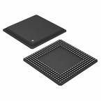
● High-Performance Fixed-Point Digital Signal Processor (TMS320C6418)
● Commercial Temperature Device
● 1.67-ns Instruction Cycle Time
● 600-MHz Clock Rate
● 4800 MIPS
● Extended Temperature Device
● 2-ns Instruction Cycle Time
● 500-MHz Clock Rate
● 4000 MIPS
● Eight 32-Bit Instructions/Cycle
● Fully Software-Compatible With C64x™
● VelociTI.2™ Extensions to VelociTI™ Advanced Very-Long-Instruction-Word (VLIW) TMS320C64x™ DSP Core
● Eight Highly Independent Functional Units With VelociTI.2™ Extensions:
● Six ALUs (32-/40-Bit), Each Supports Single 32-Bit, Dual 16-Bit, or Quad 8-Bit Arithmetic per Clock Cycle
● Two Multipliers Support Four 16 x 16-Bit Multiplies (32-Bit Results) per Clock Cycle or Eight 8 x 8-Bit Multiplies (16-Bit Results) per Clock Cycle
● Load-Store Architecture With Non-Aligned Support
● 64 32-Bit General-Purpose Registers
● Instruction Packing Reduces Code Size
● All Instructions Conditional
● Instruction Set Features
● Byte-Addressable (8-/16-/32-/64-Bit Data)
● 8-Bit Overflow Protection
● Bit-Field Extract, Set, Clear
● Normalization, Saturation, Bit-Counting
● VelociTI.2™ Increased Orthogonality
● VelociTI.2™ Extensions to VelociTI™ Advanced Very-Long-Instruction-Word (VLIW) TMS320C64x™ DSP Core
● Viterbi Decoder Coprocessor (VCP)
● Supports Over 500 7.95-Kbps AMR
● Programmable Code Parameters
● L1/L2 Memory Architecture
● 128K-Bit (16K-Byte) L1P Program Cache (Direct Mapped)
● 128K-Bit (16K-Byte) L1D Data Cache (2-Way Set-Associative)
● 4M-Bit (512K-Byte) L2 Unified Mapped RAM/Cache (Flexible RAM/Cache Allocation)
● Endianess: Little Endian, Big Endian
● 32-Bit External Memory Interface (EMIF)
● Glueless Interface to Asynchronous Memories (SRAM and EPROM) and Synchronous Memories (SDRAM, SBSRAM, ZBT SRAM, and FIFO)
● 512M-Byte Total Addressable External Memory Space
● Enhanced Direct-Memory-Access (EDMA) Controller (64 Independent Channels)
● Host-Port Interface (HPI) [32-/16-Bit]
● Two Multichannel Audio Serial Ports (McASPs) - with Six Serial Data Pins each
● Two Inter-Integrated Circuit (I2C) Buses
● Additional GPIO Capability
● Two Multichannel Buffered Serial Ports
● Three 32-Bit General-Purpose Timers
● Sixteen General-Purpose I/O (GPIO) Pins
● Flexible PLL Clock Generator
● On-Chip Fundamental Oscillator
● IEEE-1149.1 (JTAG) Boundary-Scan-Compatible
● 288-Pin Ball Grid Array (BGA) Package (GTS and ZTS Suffixes), 1.0-mm Ball Pitch
● 0.13-µm/6-Level Cu Metal Process (CMOS)
● 3.3-V I/Os, 1.4-V Internal (-600)
● 3.3-V I/Os, 1.2-V Internal (A-500)


