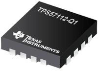
●The TPS57112-Q1 device is a full-featured 6-V, 2-A, synchronous step-down current-mode converter with two integrated MOSFETs.
●The TPS57112-Q1 device enables small designs by integrating the MOSFETs, implementing current-mode control to reduce external component count, reducing inductor size by enabling up to 2-MHz switching frequency, and minimizing the IC footprint with a small 3-mm × 3-mm thermally enhanced QFN package.
●The TPS57112-Q1 device provides accurate regulation for a variety of loads with a ±1% voltage reference (Vref) over temperature.
●The integrated 12-mΩ MOSFETs and 515-µA typical supply current maximize efficiency. Using the enable pin to enter the shutdown mode reduces supply current to 5.5 µA, typical.
●The internal undervoltage lockout setting is 2.45 V, but programming the threshold with a resistor network on the enable pin can increase the setting. The slow-start pin controls the output-voltage start-up ramp. An open-drain power-good signal indicates when the output is within 93% to 107% of its nominal voltage.
●Frequency foldback and thermal shutdown protect the device during an overcurrent condition.
●The SwitcherPro™ software tool, available at www.ti.com/tool/switcherpro, supports the TPS57112-Q1 device.
●For more SWIFT™ documentation, see the TI Web site at www.ti.com/swift.
● Qualified for Automotive Applications
● AEC-Q100 Qualified With the Following Results:
● Device Temperature Grade 1: –40°C to 125°C
●Ambient Operating Temperature Range
● Device HBM ESD Classification Level H2
● Device CDM ESD Classification Level C3B
● Two 12-mΩ (Typical) MOSFETs for High
●Efficiency at 2-A Loads
● 200-kHz to 2-MHz Switching Frequency
● 0.8 V ± 1% Voltage Reference Over Temperature
●(–40°C to 150°C)
● Synchronizes to External Clock
● Adjustable Slow Start and Sequencing
● UV and OV Power-Good Output
● –40°C to 150°C Operating Junction Temperature
●Range
● Thermally Enhanced 3-mm × 3-mm 16-Pin QFN
● Pin-Compatible to TPS54418


