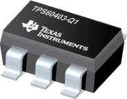
●The TPS6040x-Q1 family of devices generate an unregulated negative output voltage from an input voltage ranging from 1.8 V to 5.25 V. The devices are typically supplied by a preregulated supply rail of 5 V or 3.3 V. Due to its wide-input voltage range, two or three NiCd, NiMH, or alkaline battery cells, as well as one Li-Ion cell, can also power them.
●Only three external 1-µF capacitors are required to build a complete DC-DC charge pump inverter. Assembled in a 5-pin SOT-23 package, the complete converter can be built on a 50-mm2 board area. Replacing the Schottky diode typically needed for start-up into load with integrated circuitry can achieve additional board area and component count reduction.
●The TPS6040x-Q1 can deliver a maximum output current of 60 mA, with a typical conversion efficiency of greater than 90% over a wide output current range. Three device options TPS60401/2/3-Q1 with 20-kHz, 50-kHz, and 250-kHz fixed frequency operation are available. TPS60400-Q1 device comes with a variable switching frequency to reduce operating current in applications with a wide load range and enables the design with low-value capacitors.
● Qualified for Automotive Applications
● AEC-Q100 Test Guidance With the Following Results:
● Device Temperature Grade 1: –40°C to +125°C Ambient Operating Temperature Range
● Device HBM ESD Classification Level 2
● Device CDM ESD Classification Level C6
● Inverts Input Supply Voltage
● Up to 60-mA Output Current
● Only Three Small 1-µF Ceramic Capacitors Needed
● Input Voltage Range From 1.8 V to 5.25 V
● PowerSave-Mode for Improved Efficiency at Low Output Currents (TPS60400-Q1)
● Device Quiescent Current Typical: 100 µA
● Integrated Active Schottky-Diode for Start-Up Into Load
● Small 5-Pin SOT23 Package
● Evaluation Module Available: TPS60400EVM-178


