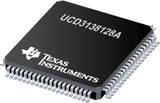
●The UCD3138xA is a digital power supply controller from Texas Instruments offering superior levels of integration and performance in a single chip solution. The UCD3138128A offers 128 kB of program flash memory in comparison to 32 kB in UCD3138A. and it also provides additional options for communication such as SPI and a second I2C/PMBus port. The availability of of program Flash memory in multiple 32 kB banks enables designers to implement dual images of firmware (that is, one main image + one back-up image) in the device and provides the option to execute from either of the banks using appropriate algorithms. It also creates the unique opportunity for the processor to load a new program and subsequently execute that program without interrupting power delivery. This feature allows the end user to add new features to the power supply in the field while eliminating any down-time required to load the new program.
●The flexible nature of the UCD3138xA family makes it suitable for a wide variety of power conversion applications. In addition, multiple peripherals inside the device have been specifically optimized to enhance the performance of AC/DC and isolated DC/DC applications and reduce the solution component count in the IT and network infrastructure space. The UCD3138xA family is a fully programmable solution offering customers complete control of their application, along with ample flexibility for many solutions. At the same time, TI is committed to simplifying our customer’s development effort through offering best in class development tools, including application firmware, Code Composer StudioTM software development environment, and TI’s Fusion Power Development GUI which enables customers to configure and monitor key system parameters.
●At the core of the controller are the Digital Power Peripherals (DPP). Each DPP implements a high speed digital control loop consisting of a dedicated Error Analog to Digital Converter (EADC), a PID based 2 pole - 2 zero digital compensator and DPWM outputs with 250 ps pulse width resolution. The device also contains a 12-bit, 539 ksps general purpose ADC with up to 15 channels, timers, interrupt control, PMBus, I2C, SPI and UART communications ports. The device is based on a 32-bit ARM7TDMI-S RISC microcontroller that performs real-time monitoring, configures peripherals and manages communications. The ARM microcontroller executes its program out of programmable flash memory as well as on chip RAM and ROM.
●In addition to the DPP, specific power management peripherals have been added to enable high efficiency across the entire operating range, high integration for increased power density, reliability, and lowest overall system cost and high flexibility with support for the widest number of control schemes and topologies. Such peripherals include: light load burst mode, synchronous rectification, LLC and phase shifted full bridge mode switching, input voltage feed forward, copper trace current sense, ideal diode emulation, constant current constant power control, synchronous rectification soft on and off, peak current mode control, flux balancing, secondary side input voltage sensing, high resolution current sharing, hardware configurable soft start with pre bias, as well as several other features. Topology support has been optimized for voltage mode and peak current mode controlled phase shifted full bridge, single and dual phase PFC, bridgeless PFC, hard switched full bridge and half bridge, active clamp forward converter, two switch forward converter and LLC half bridge and full bridge.
●The UCD3138128A is a functional variant of the UCD3138 Digital Power Controller that includes significant improvements over the UCD3138. For a description of the complete changes made in the UCD3138128A, refer to UCD3138128A Migration Guide. The major improvements are: The General Purpose ADC has been improved for better accuracy and performance at extreme cold temperatures (–40°C). The UART peripheral has been modified to include a hardware based auto-baud rate adjustment feature. A new Synchronous Rectifier Dead Time Optimization hardware peripheral has been added. Benefits include: Improved efficiency Reduced synchronous rectifier voltage stressesShorter development cycleA Duty Cycle Read Function has been added to improve use in peak current mode.


