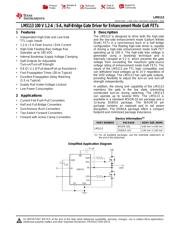
●The LM5113 is designed to drive both the high-side and the low-side enhancement mode Gallium Nitride (GaN) FETs in a synchronous buck or a half bridge configuration. The floating high-side driver is capable of driving a high-side enhancement mode GaN FET operating up to 100 V. The high-side bias voltage is generated using a bootstrap technique and is internally clamped at 5.2 V, which prevents the gate voltage from exceeding the maximum gate-source voltage rating of enhancement mode GaN FETs. The inputs of the LM5113 are TTL logic compatible, and can withstand input voltages up to 14 V regardless of the VDD voltage. The LM5113 has split gate outputs, providing flexibility to adjust the turn-on and turn-off strength independently.
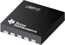
●In addition, the strong sink capability of the LM5113 maintains the gate in the low state, preventing unintended turn-on during switching. The LM5113 can operate up to several MHz. The LM5113 is available in a standard WSON-10 pin package and a 12-bump DSBGA package. The WSON-10 pin package contains an exposed pad to aid power dissipation. The DSBGA package offers a compact footprint and minimized package inductance.
● Independent High-Side and Low-Side
●TTL Logic Inputs
● 1.2 A / 5 A Peak Source / Sink Current
● High-Side Floating Bias Voltage Rail
●Operates up to 100 VDC
● Internal Bootstrap Supply Voltage Clamping
● Split Outputs for Adjustable
●Turn-on/Turn-off Strength
● 0.6 Ω / 2.1 Ω Pull-down/Pull-up Resistance
● Fast Propagation Times (28 ns Typical)
● Excellent Propagation Delay Matching
●(1.5 ns Typical)
● Supply Rail Under-Voltage Lockout
● Low Power Consumption


