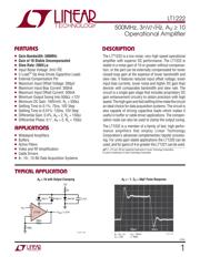
Web Analytics
Part Datasheet Search > Operational Amplifiers(General Purpose) > LT1222 Datasheet PDF
Images are for reference

LT1222 Datasheet PDF

Part Series:
LT1222 Series
Category:
Operational Amplifiers(General Purpose)
Description:
LINEAR TECHNOLOGY LT1222CN8#PBF Operational Amplifier, Single, 1 Amplifier, 500MHz, 200V/µs, ± 5V to ± 15V, DIP, 8Pins
Updated Time: 2023/09/27 08:49:05 (UTC + 8)

LT1222 Operational Amplifiers(General Purpose) Datasheet PDF

LT1222 Datasheet PDF Operational Amplifiers(General Purpose)

12 Pages
Linear Technology
IC OP-AMP 500MHz 200V/US 8-DIP
12 Pages
ADI
500MHz, 3nV/√Hz, AV ≥ 10 Operational Amplifier
12 Pages
Linear Technology
IC OP-AMP 500MHz 200V/US 8-SOIC
12 Pages
Linear Technology
IC OP-AMP 500MHz 200V/US 8-SOIC
12 Pages
Linear Technology
IC OP-AMP 500MHz 200V/US 8-SOIC
12 Pages
ADI
500MHz, 3nV/√Hz, AV ≥ 10 Operational Amplifier
12 Pages
ADI
500MHz, 3nV/√Hz, AV ≥ 10 Operational Amplifier
12 Pages
ADI
500MHz, 3nV/√Hz, AV ≥ 10 Operational Amplifier
12 Pages
Linear Technology
OP Amp Single GP ±18V 8Pin CDIP N
12 Pages
ADI
500MHz, 3nV/√Hz, AV ≥ 10 Operational Amplifier
12 Pages
ADI
Operational Amplifier, 1 Func, 600uV Offset-Max, BIPolar, PDSO8
12 Pages
Linear Technology
IC OPAMP GP 500MHz 8SO
12 Pages
Linear Technology
IC OPAMP GP 500MHz 8SO
12 Pages
ADI
Operational Amplifier, 1 Func, 600uV Offset-Max, BIPolar, PDIP8
12 Pages
ADI
Operational Amplifier, 1 Func, 600uV Offset-Max, BIPolar, PDSO8

LT1222CN8#PBF - Linear Technology Specifications

TYPE
DESCRIPTION
Mounting Style
Through Hole
Number of Pins
8 Pin
Supply Voltage (DC)
18.0 V
Case/Package
DIP-8
Supply Current
8 mA
show more

LT1222CN8#PBF - Linear Technology Function Overview

The LT1222CN8#PBF is a 500MHz very high speed Operational Amplifier with superior DC performance. The LT1222 is stable in a noise gain of 10 or greater without compensation or the part can be externally compensated for lower closed-loop gain at the expense of lower bandwidth and slew rate. This low noise amplifier features reduced input offset voltage, lower input bias currents, lower noise and higher DC gain than devices with comparable bandwidth and slew rate. The circuit is a single gain stage that includes proprietary DC gain enhancement circuitry to obtain precision with high speed. The high gain and fast settling time make the circuit an ideal choice for data acquisition systems. The circuit is also capable of driving capacitive loads which makes it useful in buffer or cable driver applications. The compensation node can also be used to clamp the output swing.
Gain of 10 stable uncompensated
3nV/√Hz Input noise voltage
C-Load™ operational amplifier drives all capacitive loads
External compensation pin
300µV Maximum input offset voltage
300nA Maximum input bias current
300nA Maximum input offset current
±12V Minimum output swing into 500R
100V/mV Minimum DC gain (RL = 500R)
75ns Settling time to 0.1%, 10V step
120ns Settling time to 0.01%, 10V step
0.4% Differential gain (AV = 2, RL = 150R)
0.1° Differential phase (AV = 2, RL = 150R)
show more
Part Datasheet PDF Search
Loading...
72,405,303 Parts Datasheet PDF, Update more than 5,000 PDF files ervery day.

Relate Parts