Web Analytics
Part Datasheet Search > Hot Swap & Power Distribution > TPS2041 Datasheet PDF
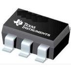
Images are for reference

TPS2041 Datasheet PDF

Part Series:
TPS2041 Series
Category:
Hot Swap & Power Distribution
Description:
USB Power SW Hi Side/DIST Single 2.7V to 5.5V 0.75A to 1.25A 5Pin SOT-23 T/R
Updated Time: 2023/01/13 02:37:25 (UTC + 8)

TPS2041 Datasheet PDF Hot Swap & Power Distribution

60 Pages
TI
USB Power SW USB Power Switch Single 5.5V 0.75A to 1.25A 8Pin HVSSOP EP T/R
60 Pages
TI
USB Power Switch Single 5.5V 0.75A to 1.25A 5Pin SOT-23 T/R
60 Pages
TI
USB Power Switch Single 5.5V 0.75A to 1.25A 8Pin HVSSOP EP Tube
60 Pages
TI
USB Power Switch Single 5.5V 0.75A to 1.25A 8Pin HVSSOP EP T/R
60 Pages
TI
USB Power Switch Single 5.5V 0.75A to 1.25A 8Pin HVSSOP EP Tube
40 Pages
TI
USB Power SW DIST Single 5.5V 0.85A 5Pin SOT-23 T/R
40 Pages
TI
USB Power SW DIST Single 5.5V 0.85A 5Pin SOT-23 T/R
34 Pages
TI
USB Power Switch Single 5.5V 0.9A 8Pin SOIC T/R
34 Pages
TI
USB Power Switch Single 5.5V 0.9A 8Pin SOIC Tube
34 Pages
TI
USB Power SW USB Power Switch Single 5.5V 0.9A 8Pin SOIC T/R
34 Pages
TI
USB Power SW USB Power Switch Single 5.5V 0.9A 8Pin SOIC T/R
31 Pages
TI
USB Power Switch Single 5.5V 1A Automotive 5Pin SOT-23 T/R
25 Pages
TI
USB Power SW USB Power Switch Single 5.5V 0.9A 8Pin SOIC Tube
25 Pages
TI
USB Power Switch Single 5.5V 1A 5Pin SOT-23 T/R
25 Pages
TI
USB Power Switch Single 5.5V 0.9A 8Pin PDIP Tube
25 Pages
TI
USB Power Switch Single 5.5V 0.9A 8Pin SOIC T/R

TPS2041BDBVR - TI Specifications

TYPE
DESCRIPTION
Mounting Style
Surface Mount
Number of Pins
5 Pin
Supply Voltage (DC)
5.00 V
Case/Package
SOT-23-5
Number of Outputs
1 Output
show more

TPS2041BDBVR - TI Function Overview

The TPS2041BDBVR is a 1-channel Current Limited Power Distribution Switch intended for applications where heavy capacitive loads and short-circuits are likely to be encountered. This device incorporates 70mR N-channel MOSFET power switches for power-distribution systems that require multiple power switches. Each switch is controlled by a logic enable input. Gate drive is provided by an internal charge pump designed to control the power-switch rise times and fall times to minimize current surges during switching. The charge pump requires no external components. When the output load exceeds the current-limit threshold or a short is present, the device limits the output current to a safe level by switching into a constant-current mode, pulling the over-current logic output low. When continuous heavy overloads and short-circuits increase the power dissipation in the switch, causing the junction temperature to rise, a thermal protection circuit shuts off the switch to prevent damage.
70mR High-side MOSFET
500mA Continuous current
Thermal and short-circuit protection
Accurate current limit (0.75A minimum, 1.25A maximum)
2.7 to 5.5V Operating range
0.6ms Typical rise time
Under-voltage lockout
Deglitched fault report (OC)
No OC glitch during power up
1µA Maximum standby supply current
Green product and no Sb/Br
This device has limited built-in ESD protection, leads should be shorted together or the device placed in conductive foam during storage or handling to prevent electrostatic damage to the MOS gates.
show more
Part Datasheet PDF Search
Loading...
72,405,303 Parts Datasheet PDF, Update more than 5,000 PDF files ervery day.

Relate Parts