Web Analytics
Part Datasheet Search > Logic ICs > 74LVC16245 Datasheet PDF
Images are for reference

74LVC16245 Datasheet PDF

Part Series:
74LVC16245 Series
Category:
Logic ICs
Description:
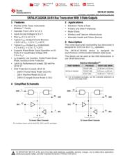
16Bit Bus Transceiver With 3-State Outputs 48-TSSOP -40℃ to 125℃
Updated Time: 2023/01/13 03:19:50 (UTC + 8)

74LVC16245 Datasheet PDF Logic ICs

21 Pages
NXP
Bus XCVR Dual 16CH 3-ST 48Pin SSOP T/R
21 Pages
Nexperia
IC BUS TRCVR 3-ST 16Bit 48TSSOP
21 Pages
Nexperia
IC BUS TRCVR 3-ST 16Bit 48SSOP
21 Pages
NXP
Bus XCVR Dual 16CH 3-ST 48Pin SSOP Bulk
21 Pages
Nexperia
IC BUS TRCVR 3-ST 16Bit 48SSOP
21 Pages
Nexperia
IC BUS TRCVR 3-ST 16Bit 48TSSOP
21 Pages
Nexperia
IC BUS TXRX TRI-ST 16Bit 48TSSOP
20 Pages
NXP
Bus XCVR Dual 16CH 3-ST 48Pin SSOP Tube
20 Pages
NXP
Bus XCVR Dual 16CH 3-ST Automotive 48Pin TSSOP T/R
20 Pages
NXP
IC BUS TRCVR 3-ST 16Bit 48SSOP
20 Pages
NXP
Bus XCVR Dual 16CH 3-ST 56Pin VFBGA Tray
20 Pages
NXP
Bus XCVR Dual 16CH 3-ST Automotive 56Pin VFBGA T/R
17 Pages
Integrated Device Technology
Bus Transceiver, LVC/LCX/Z Series, 2-Func, 8Bit, True Output, CMOS, PDSO48, 0.635MM PITCH, SSOP-48
7 Pages
Integrated Device Technology
3.3V CMOS 16Bit Bus Transceiver with 3-State Outputs and 5V Tolerant I/O
6 Pages
Integrated Device Technology
3.3V CMOS 16Bit Bus Transceiver with 3-State Outputs and 5V Tolerant I/O
6 Pages
Integrated Device Technology
3.3V CMOS 16Bit Bus Transceiver with 3-State Outputs and 5V Tolerant I/O

74LVC16245ADGGRG4 - TI Specifications

TYPE
DESCRIPTION
Mounting Style
Surface Mount
Number of Pins
48 Pin
Supply Voltage (DC)
1.65V ~ 3.60V
Case/Package
TSSOP-48
Number of Outputs
16 Output
show more

74LVC16245ADGGRG4 - TI Function Overview

DESCRIPTION/ORDERING INFORMATION
This 16-bit (dual-octal) noninverting bus transceiver is designed for 1.65-V to 3.6-V VCC operation. The SN74LVC16245A is designed for asynchronous communication between data buses. The control-function implementation minimizes external timing requirements. This device can be used as two 8-bit transceivers or one 16-bit transceiver. It allows data transmission from the A bus to the B bus or from the B bus to the A bus, depending on the logic level at the direction-control (DIR) input. The output-enable (OE) input can be used to disable the device so that the buses are effectively isolated.
To ensure the high-impedance state during power up or power down, OE should be tied to VCC
through a pullup resistor; the minimum value of the resistor is determined by the current-sinking capability of the driver.
FEATURES
• Member of the Texas Instruments Widebus™ Family
• Operates From 1.65 V to 3.6 V
• Inputs Accept Voltages to 5.5 V
• Max tpd of 4 ns at 3.3 V
• Typical VOLP (Output Ground Bounce)
  <0.8 V at VCC = 3.3 V, TA = 25°C
• Typical VOHV (Output VOH Undershoot)
   >2 V at VCC = 3.3 V, TA = 25°C
• Supports Mixed-Mode Signal Operation on All Ports (5-V Input/Output Voltage With 3.3-V VCC)
• Ioff Supports Partial-Power-Down Mode Operation
• Latch-Up Performance Exceeds 250 mA Per JESD 17
• ESD Protection Exceeds JESD 22
– 2000-V Human-Body Model (A114-A)
– 200-V Machine Model (A115-A)
– 1000-V Charged-Device Model (C101)
show more
Part Datasheet PDF Search
Loading...
72,405,303 Parts Datasheet PDF, Update more than 5,000 PDF files ervery day.

Relate Parts