●Product Details
●### For a limited time, take a live test drive of the AD6676 by using our remote evaluation software.
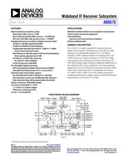
●The AD6676 is a highly integrated IF subsystem that can digitize radio frequency (RF) bands up to 160 MHz in width centered on an intermediate frequency (IF) of 70 MHz to 450 MHz. Unlike traditional Nyquist IF sampling ADCs, the AD6676 relies on a tunable band-pass Σ-Δ ADC with a high oversampling ratio to eliminate the need for band specific IF SAW filters and gain stages, resulting in significant simplification of the wideband radio receiver architecture. On-chip quadrature digital downconversion followed by selectable decimation filters reduces the complex data rate to a manageable rate between 62.5 MSPS to 266.7 MSPS. The 16-bit complex output data is transferred to the host via a single or dual lane JESD204B interface supporting line rates of up to 5.333 Gbps.
●Applications
● Wideband cellular infrastructure equipment and repeaters
● Point-to-point microwave equipment
● Instrumentation
● Spectrum and communication analyzers
● Software defined radio
●### Features and Benefits
● High instantaneous dynamic range
● Noise figure (NF) as low as 13 dB
● Noise spectral density (NSD) as low as −159 dBFS/Hz
● IIP3 up to 36.9 dBm with spurious tones <−99 dBFS
● Tunable band-pass Σ-Δ analog-to-digital converter (ADC)
● 20 MHz to 160 MHz signal bandwidth
● 70 MHz to 450 MHz IF center frequency
● Configurable input full-scale level of −2 dBm to −14 dBm
● Easy to drive resistive IF input
● Gain flatness of 1 dB with under 0.5 dB out-of-band peaking
● Alias rejection greater than 50 dB
● 2.0 GSPS to 3.2 GSPS ADC clock rate
● On-chip PLL clock multiplier
● 16-bit I/Q rate up to 266 MSPS
● On-chip digital signal processing
● NCO and quadrature digital downconverter (QDDC)
● Selectable decimation factor of 12, 16, 24, and 32
● Automatic gain control (AGC) support
● On-chip attenuator with 27 dB span in 1 dB steps
● Fast attenuator control via configurable AGC data port
● Peak detection flags with programmable thresholds
● Single or dual lane, JESD204B capable
● Low power consumption: 1.20 W
● 1.1 V and 2.5 V supply voltage
● TDD power saving up to 60%
● 4.3 mm × 5.0 mm WLCSP