Web Analytics
Part Datasheet Search > Operational Amplifiers(General Purpose) > AD648 Datasheet PDF
Images are for reference

AD648 Datasheet PDF

Part Series:
AD648 Series
Category:
Operational Amplifiers(General Purpose)
Description:
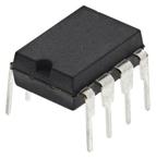
ANALOG DEVICES AD648JNZ Operational Amplifier, Dual, 2 Amplifier, 1MHz, 1.8V/µs, ± 4.5V to ± 18V, DIP, 8Pins
Updated Time: 2023/09/27 08:34:10 (UTC + 8)

AD648 Operational Amplifiers(General Purpose) Datasheet PDF

AD648 Datasheet PDF Operational Amplifiers(General Purpose)

21 Pages
ADI
IC OPAMP BIFET 1MHz DUAL 8SOIC
16 Pages
ADI
ANALOG DEVICES AD648KNZ Operational Amplifier, Dual, 2 Amplifier, 1MHz, 1.8V/µs, ± 4.5V to ± 18V, DIP, 8Pins
14 Pages
ADI
ANALOG DEVICES AD648JNZ Operational Amplifier, Dual, 2 Amplifier, 1MHz, 1.8V/µs, ± 4.5V to ± 18V, DIP, 8Pins
14 Pages
ADI
IC OPAMP JFET 1MHz 8SOIC
14 Pages
ADI
IC OPAMP JFET 1MHz 8SOIC
14 Pages
ADI
IC OPAMP JFET 1MHz 8SOIC
13 Pages
ADI
ANALOG DEVICES AD648KRZ Operational Amplifier, Dual, 2 Amplifier, 1MHz, 1.8V/µs, ± 4.5V to ± 18V, SOIC, 8Pins
13 Pages
ADI
IC DUAL OP-AMP, 300uV OFFSET-MAX, 1MHz BAND WIDTH, MBCY8, HERMETIC SEALED, METAL CAN, TO-99, 8Pin, Operational Amplifier
12 Pages
ADI
IC OPAMP BIFET 1MHz DUAL 8SOIC
12 Pages
ADI
OP Amp Dual GP ±18V 8Pin TO-99
12 Pages
ADI
IC OPAMP BIFET 1MHz DUAL 8SOIC
12 Pages
ADI
OP Amp Dual GP ±18V 8Pin CDIP
12 Pages
ADI
OP Amp Dual GP ±18V 8Pin CDIP
12 Pages
ADI
IC OPAMP JFET 1MHz 8SOIC
12 Pages
ADI
IC OPAMP BIFET 1MHz DUAL 8SOIC
12 Pages
ADI
IC OPAMP BIFET 1MHz DUAL 8SOIC

AD648JNZ - ADI Specifications

TYPE
DESCRIPTION
Mounting Style
Through Hole
Number of Pins
8 Pin
Supply Voltage (DC)
15.0 V
Operating Voltage
4.5V ~ 18V
Case/Package
DIP-8
show more

AD648JNZ - ADI Function Overview

The AD648JNZ is a precision low power dual BiFET Operational Amplifier offers both low bias current (10pA maximum, warmed up) and low quiescent current (400µA maximum) and is fabricated with ion-implanted FET and laser wafer trimming technologies. Input bias current is guaranteed over the AD648"s entire common-mode voltage range. The economical J grade has a maximum guaranteed offset voltage of less than 2mV and an offset voltage drift of less than 20µV/°C. This level of DC precision is achieved using Analog"s laser wafer drift trimming process. The combination of low quiescent current and low offset voltage drift minimizes changes in input offset voltage due to self-heating effects. The AD648 is recommended for any dual supply op amp application requiring low power and excellent DC and AC performance. In applications such as battery-powered, precision instrument front ends and CMOS DAC buffers.
Pin compatible with industry standard dual op amps such as the LF442 and TL062
Indefinite output short-circuit duration
400µA Maximum quiescent current
500mW Internal power dissipation
ESD sensitive device, electrostatic charges as high as 4000V readily accumulate on the human body and test equipment and can discharge without detection.
show more
Part Datasheet PDF Search
Loading...
72,405,303 Parts Datasheet PDF, Update more than 5,000 PDF files ervery day.
Relate Parts