Web Analytics
Part Datasheet Search > Clock & Timing > AD9516 Datasheet PDF
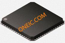
Images are for reference

AD9516 Datasheet PDF

Part Series:
AD9516 Series
Category:
Clock & Timing
Description:
Clock Generator -40℃ to 85℃ 64Pin LFCSP EP Tray
Updated Time: 2023/01/13 02:53:15 (UTC + 8)

AD9516 Datasheet PDF Clock & Timing

81 Pages
ADI
Clock Generator -40℃ to 85℃ 64Pin LFCSP EP Tray
81 Pages
ADI
ANALOG DEVICES AD9516-2BCPZ Clock Generator, 2.335GHz, 3.135V-3.465V supply, 14Outputs, LFCSP-64
81 Pages
ADI
Clock Generator -40℃ to 85℃ 64Pin LFCSP EP T/R
81 Pages
ADI
Clock Generator -40℃ to 85℃ 64Pin LFCSP EP T/R
81 Pages
ADI
ANALOG DEVICES AD9516-1/PCBZ Evaluation Board, Clock IC, 2.5GHz On-Chip VCO, AD9516-1
81 Pages
ADI
ANALOG DEVICES AD9516-3/PCBZ Evaluation Board, Clock IC, 2GHz On-Chip VCO, AD9516
81 Pages
ADI
Clock Generator -40℃ to 85℃ 64Pin LFCSP EP T/R
81 Pages
ADI
ANALOG DEVICES AD9516-4/PCBZ Evaluation Board, Clock IC, 1.8GHz On-Chip VCO, AD9516-4
80 Pages
ADI
Clock Generator -40℃ to 85℃ 64Pin LFCSP EP Tray
80 Pages
ADI
Clock Generator -40℃ to 85℃ 64Pin LFCSP EP T/R
80 Pages
ADI
ANALOG DEVICES AD9516-2/PCBZ CLOCK IC WITH 2.25GHz ON=CHIP VCO
80 Pages
ADI
ANALOG DEVICES AD9516-5/PCBZ CLOCK IC WITH 2.5GHz ON-CHIP VCO EB
80 Pages
ADI
14-Output Clock Generator with Integrated 2GHz VCO
80 Pages
ADI
14-Output Clock Generator with Integrated 1.6GHz VCO
78 Pages
ADI
Clock Generator 0MHz to 250MHz-IN 2950MHz-OUT 64Pin LFCSP EP Tray
76 Pages
ADI
Clock Generator 0MHz to 250MHz-IN 2950MHz-OUT 64Pin LFCSP EP T/R

AD9516-4BCPZ - ADI Specifications

TYPE
DESCRIPTION
Mounting Style
Surface Mount
Frequency
1.8 GHz
Number of Pins
64 Pin
Supply Voltage (DC)
3.13V (min)
Case/Package
LFCSP-64
show more

AD9516-4BCPZ - ADI Function Overview

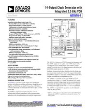
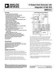
The AD9516-4BCPZ is a 14-output Clock Generator with 1.6GHz integrated voltage-controlled oscillator (VCO). The AD9516-4BCPZ provides a multi-output clock distribution function with sub pico second jitter performance, along with an on-chip PLL and VCO. The on-chip VCO tunes from 1.45 to 1.80GHz. Optionally, an external VCO/VCXO of up to 2.4GHz can be used. It emphasizes low jitter and phase noise to maximize data converter performance and it can benefit other applications with demanding phase noise and jitter requirements. It features six LVPECL outputs (in 3-pairs) and four LVDS outputs (in 2-pairs). Each LVDS output can be reconfigured as two CMOS outputs. The LVPECL outputs operate to 1.6GHz, the LVDS outputs operate to 800MHz and the CMOS outputs operate to 250MHz. Each pair of outputs has dividers that allow both the divide ratio and coarse delay (or phase) to be set. The range of division for the LVPECL outputs is 1 to 32.
Low phase noise, phase-locked loop (PLL)
On-chip VCO tunes from 1.45 to 1.80GHz
External VCO/VCXO to 2.4GHz optional
Reference monitoring capability
Automatic reverie and manual reference switchover/holdover modes
Programmable delays in path to PFD
Digital or analogue lock detect, selectable
Each output pair shares a 1-to-32 divider with coarse phase delay
Channel-to-channel skew paired outputs of <10ps
Each LVDS output can be reconfigured as two 250MHz CMOS outputs
Automatic synchronization of all outputs on power-up
Manual output synchronization available
1 Differential or 2 single-ended reference inputs
show more
Part Datasheet PDF Search
Loading...
72,405,303 Parts Datasheet PDF, Update more than 5,000 PDF files ervery day.
Relate Parts