●Product Details
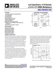
●The ADG1208 and ADG1209 are monolithic, iCMOS® analog multiplexers comprising eight single channels and four differential channels, respectively. The ADG1208 switches one of eight inputs to a common output as determined by the 3-bit binary address lines A0, A1, and A2. The ADG1209 switches one of four differential inputs to a common differential output as determined by the 2-bit binary address lines A0 and A1. An EN input on both devices enable or disable the device. When disabled, all channels are switched off. When on, each channel conducts equally well in both directions and has an input signal range that extends to the supplies.
●The iCMOS (industrial CMOS) modular manufacturing process combines high voltage CMOS (complementary metal-oxide semiconductor) and bipolar technologies. It enables the development of a wide range of high performance analog ICs capable of 33 V operation in a footprint that no other generation of high voltage devices has been able to achieve. Unlike analog ICs using conventional CMOS processes, iCMOS components can tolerate high supply voltages while providing increased performance, dramatically lower power consumption, and reduced package size.
●The ultralow capacitance and exceptionally low charge injection of these multiplexers make them ideal solutions for data acquisition and sample-and-hold applications, where low glitch and fast settling are required. There is minimum charge injection over the entire signal range of the device. iCMOS construction also ensures ultralow power dissipation, making the ds ideally suited for portable and battery-powered instruments.
●Applications
● Audio and video routing
● Automatic test equipment
● Data-acquisition systems
● Battery-powered systems
● Sample-and-hold systems
● Communication systems
●### Features and Benefits
● <1 pC charge injection over full signal range
● 1 pF off capacitance
● 33 V supply range
● 120 Ω on resistance
● Fully specified at ±15 V/+12 V
● 3 V logic compatible inputs
● Rail-to-rail operation
● Break-before-make switching action
● Available in a 16-lead TSSOP, a 16-lead LFCSP_WQ, and a 16-lead SOIC
● Typical power consumption < 0.03 μW