●Product Details
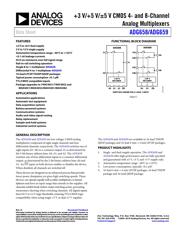
●The ADG658 and ADG659 are low voltage, CMOS analog multiplexers comprised of eight single channels and four differential channels, respectively. The ADG658 switches one of eight inputs (S1–S8) to a common output, D, as determined by the 3-bit binary address lines A0, A1, and A2. The ADG659 switches one of four differential inputs to a common differential output, as determined by the 2-bit binary address lines A0 and A1. An EN input on both devices enables or disables the device. When disabled, all channels are switched off.
●These devices are designed on an enhanced process that provides lower power dissipation yet gives high switching speeds. These devices can operate equally well as either multiplexers or demultiplexers and have an input range that extends to the supplies. All channels exhibit break-before-make switching action, preventing momentary shorting when switching channels. All digital inputs have 0.8 V to 2.4 V logic thresholds, ensuring TTL/CMOS logic compatibility when using single +5 V or dual ±5 V supplies.
●The ADG658 and ADG659 are available in 16-lead TSSOP/QSOP packages and 16-lead 4 mm × 4 mm LFCSP packages.
●Product Highlights
● 1. Single- and dual-supply operation. The ADG658 and ADG659 offer high performance and are fully specified and guaranteed with ±5 V, +5 V, and +3 V supply rails.
● 2. Automotive temperature range −40°C to +125°C.
● 3. Low power consumption, typically <0.1 μW.
● 4. 16-lead 4 mm × 4 mm LFCSP packages, 16-lead TSSOP package and 16-lead QSOP package.
●Applications
● Automotive applications
● Automatic test equipment
● Data acquisition systems
● Battery-powered systems
● Communication systems
● Audio and video signal routing
● Relay replacement
● Sample-and-hold systems
● Industrial control systems
●### Features and Benefits
● ±2 V to ±6 V dual supply
● 2 V to 12 V single supply
● Automotive temperature range −40°C to +125°C
● <0.1 nA leakage currents
● 45 Ω on resistance over full signal range
● Rail-to-rail switching operation
● Differential 4-to-1 multiplexer
● 16-lead LFCSP/TSSOP/QSOP packages
● Typical power consumption <0.1 μW
● TTL/CMOS compatible inputs
● Package upgrades to 74HC4051 / 74HC4052 and MAX4051 / MAX4052 / MAX4581 / MAX4582