Part Datasheet Search > RAM Memory > CY7C185 Datasheet PDF
Images are for reference
CY7C185 Datasheet PDF
Part Series:
CY7C185 Series
Category:
RAM Memory
Description:
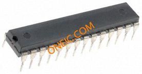
CYPRESS SEMICONDUCTOR CY7C185-20PXC SRAM, 64Kbit, 8K x 8Bit, 4.5V to 5.5V, DIP, 28Pins, 20ns
Updated Time: 2023/01/13 03:21:38 (UTC + 8)
CY7C185 RAM Memory Datasheet PDF
CY7C185 Datasheet PDF RAM Memory
35 Pages
Cypress Semiconductor
SRAM Chip Async Single 5V 64Kbit 8K x 8 20ns 28Pin CDIP
18 Pages
Cypress Semiconductor
CYPRESS SEMICONDUCTOR CY7C185-20PXC SRAM, 64Kbit, 8K x 8Bit, 4.5V to 5.5V, DIP, 28Pins, 20ns
18 Pages
Cypress Semiconductor
SRAM Chip Async Single 5V 64Kbit 8K x 8 20ns 28Pin SOJ
18 Pages
Cypress Semiconductor
SRAM Chip Async Single 5V 64Kbit 8K x 8 15ns 28Pin SOJ
18 Pages
Cypress Semiconductor
SRAM Chip Async Single 5V 64Kbit 8K x 8 15ns 28Pin SOJ
18 Pages
Cypress Semiconductor
SRAM Chip Async Single 5V 64Kbit 8K x 8 35ns 28Pin SOIC
18 Pages
Cypress Semiconductor
SRAM Chip Async Single 5V 64Kbit 8K x 8 15ns 28Pin SOJ T/R
Part Datasheet PDF Search
72,405,303 Parts Datasheet PDF, Update more than 5,000 PDF files ervery day.
