●Product Details
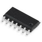
●The AD7952 is a 14-bit, charge redistribution, successive approximation register (SAR) architecture analog-to-digital converter (ADC) fabricated on Analog Devices, Inc.’s __iCMOS high voltage process. The device is configured through hardware or via a dedicated write-only serial configuration port for input range and operating mode. The AD7952 contains a high speed 14-bit sampling ADC, an internal conversion clock, an internal reference (and buffer), error correction circuits, and both serial and parallel system interface ports. A falling edge on CNVST samples the fully differential analog inputs on IN+ and IN−. The AD7952 features four different analog input ranges and three different sampling modes: warp mode for the fastest throughput, normal mode for the fastest asynchronous throughput, and impulse mode where power is scaled with throughput. Operation is specified from −40°C to +85°C.
●Applications
● Process controls Medical instruments
● High speed data acquisition
● Digital signal processing
● Instrumentation
● Spectrum analysis
● ATE
●### Features and Benefits
● Multiple pins/software-programmable input ranges
●+5 V (10 V p-p), +10 V (20 V p-p),
●±5 V (20 V p-p), ±10 V (40 V p-p)
● Pins or serial SPI®-compatible input ranges/mode selection
● Throughput
●1 MSPS (warp mode)
●800 kSPS (normal mode)
●670 kSPS (impulse mode)
● 14-bit resolution with no missing codes
● INL: ±0.3 LSB typical, ±1 LSB maximum (±61 ppm of FSR)
● _SNR: 85 dB @ 2 kHz_
● _i_CMOS® process technology
● 5 V internal reference: typical drift 3 ppm/°C; TEMP output
● No pipeline delay (SAR architecture)
● Parallel (14- or 8-bit bus) and serial 5 V/3.3 V interface
● SPI-/QSPI™-/MICROWIRE™-/DSP-compatible
● Power dissipation
●235 mW @ 1 MSPS
●10 mW @ 1 kSPS

 Part 3D Model
