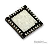
●Product Details
●The ADL5240 is a high performance, digitally controlled variable gain amplifier (VGA) operating from 100 MHz to 4000 MHz. The VGA integrates a high performance, 20 dB gain, internally matched amplifier (AMP) with a 6-bit digital step attenuator (DSA) that has a gain control range of 31.5 dB in 0.5 dB steps with ±0.25 dB step accuracy. The attenuation of the DSA can be controlled using a serial or parallel interface.
●Both the gain block and DSA are internally matched to 50 Ω at their inputs and outputs and are separately biased. The separate bias allows all or part of the ADL5240 to be used, which facilitates easy reuse throughout a design. The pinout of the ADL5240 also enables either the gain block or DSA to be first, giving the VGA maximum flexibility in a signal chain.
●The ADL5240 consumes just 93 mA and operates from a single supply ranging from 4.75 V to 5.25 V. The VGA is packaged in a thermally efficient, 5 mm × 5 mm, 32-lead LFCSP and is fully specified for operation from −40°C to +85°C. A fully populated evaluation board is available.
●Applications
● Wireless infrastructure
● Automated test equipment
● RF/IF gain control
●### Features and Benefits
● Operating frequency from 100 MHz to 4000 MHz
● Digitally controlled VGA with serial and parallel interfaces
● 6-bit, 0.5 dB digital step attenuator
● 31.5 dB gain control range with ±0.25 dB step accuracy
● Gain block or digital step attenuator can be first
● Single supply operation from 4.75 V to 5.25 V
● 31.5 dB gain control range with ±0.25 dB step accuracy
● Gain block amplifier specifications
● Gain: 19.7 dB at 2.14 GHz
● OIP3: 41.0 dBm at 2.14 GHz
● P1dB: 19.5 dBm at 2.14 GHz
● Noise figure: 2.9 dB at 2.14 GHz
● Low quiescent current of 93 mA
● Thermally efficient, 5 mm × 5 mm, 32-lead LFCSP
● The companion ADL5243 integrates a ¼ W driver amplifier to the output of the gain block and DSA

 Part 3D Model
