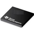
●Description
●The OMAP-L138 C6000 DSP+ARM processor is a low-power applications processor based on an ARM926EJ-S and a C674x DSP core. This processor provides significantly lower power than other members of the TMS320C6000™ platform of DSPs.
●OMAP-L138 C6000 DSP+ARM Processor
●Features
●• Dual-Core SoC
●– 375- and 456-MHz ARM926EJ-S™ RISC MPU
●– 375- and 456-MHz C674x Fixed- and Floating Point VLIW DSP
●• ARM926EJ-S Core
●– 32- and 16-Bit ( Thumb®) Instructions
●– DSP Instruction Extensions
●– Single-Cycle MAC
●– ARM Jazelle® Technology
●– Embedded ICE-RT™ for Real-Time Debug
●• ARM9™ Memory Architecture
●– 16KB of Instruction Cache
●– 16KB of Data Cache
●– 8KB of RAM (Vector Table)
●– 64KB of ROM
●• C674x Instruction Set Features
●– Superset of the C67x+ and C64x+ ISAs
●– Up to 3648 MIPS and 2746 MFLOPS
●– Byte-Addressable (8-, 16-, 32-, and 64-Bit Data)
●– 8-Bit Overflow Protection
●– Bit-Field Extract, Set, Clear
●– Normalization, Saturation, Bit-Counting
●– Compact 16-Bit Instructions
●• C674x Two-Level Cache Memory Architecture
●– 32KB of L1P Program RAM/Cache
●– 32KB of L1D Data RAM/Cache
●– 256KB of L2 Unified Mapped RAM/Cache
●– Flexible RAM/Cache Partition (L1 and L2)
●• Enhanced Direct Memory Access Controller 3(EDMA3):
●– 2 Channel Controllers
●– 3 Transfer Controllers
●– 64 Independent DMA Channels
●– 16 Quick DMA Channels
●– Programmable Transfer Burst Size
●• TMS320C674x Floating-Point VLIW DSP Core
●– Load-Store Architecture with Nonaligned Support
●– 64 General-Purpose Registers (32-Bit)
●– Six ALU (32- and 40-Bit) Functional Units
●• Supports 32-Bit Integer, SP (IEEE Single Precision/32-Bit) and DP (IEEE Double Precision/64-Bit) Floating Point
●• Supports up to Four SP Additions Per Clock, Four DP Additions Every Two Clocks
●• Supports up to Two Floating-Point (SP or DP) Reciprocal Approximation (RCPxP) and Square-Root Reciprocal Approximation (RSQRxP) Operations Per Cycle
●– Two Multiply Functional Units:
●• Mixed-Precision IEEE Floating-Point Multiply Supported up to:
●– 2 SP x SP → SP Per Clock
●– 2 SP x SP → DP Every Two Clocks
●– 2 SP x DP → DP Every Three Clocks
●– 2 DP x DP → DP Every Four Clocks
●• Fixed-Point Multiply Supports Two 32 x 32-Bit Multiplies, Four 16 x 16-Bit Multiplies, or Eight 8 x 8-Bit Multiplies per Clock Cycle, and Complex Multiples
●– Instruction Packing Reduces Code Size
●– All Instructions Conditional
●– Hardware Support for Modulo Loop Operation
●– Protected Mode Operation
●– Exceptions Support for Error Detection and Program Redirection
●Software Support
●– TI DSP BIOS™
●– Chip Support Library and DSP Library
●128KB of RAM Shared Memory
●1.8-V or 3.3-V LVCMOS I/Os (Except for USB and DDR2 Interfaces)
●Two External Memory Interfaces:
●– EMIFA
● • NOR (8- or 16-Bit-Wide Data)
● • NAND (8- or 16-Bit-Wide Data)
● • 16-Bit SDRAM with 128-MB Address Space
●– DDR2/Mobile DDR Memory Controller with one of the following:
● • 16-Bit DDR2 SDRAM with 256-MB Address Space
●Applications
●• Professional or Private Mobile Radio (PMR)
●• Remote Radio Unit (RRU)
●• Remote Radio Head (RRH)
●• Industrial Automation
●• Currency Inspection
●• Biometric Identification
●• Machine Vision (Low-End)
●• Smart Grid Substation Protection
●• Industrial Portable Navigation Devices


