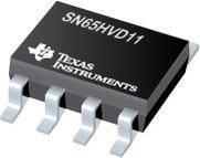
●The SN65HVD10, SN75HVD10, SN65HVD11, SN75HVD11, SN65HVD12, and SN75HVD12 bus transceivers combine a 3-state differential line driver and differential input line receiver that operate with a single 3.3-V power supply. They are designed for balanced transmission lines and meet or exceed ANSI standard TIA/EIA-485-A and ISO 8482:1993. These differential bus transceivers are monolithic integrated circuits designed for bidirectional data communication on multipoint bus-transmission lines. The drivers and receivers have active-high and active-low enables, respectively, that can be externally connected together to function as direction control. Very low device standby supply current can be achieved by disabling the driver and the receiver.
●The driver differential outputs and receiver differential inputs connect internally to form a differential input/ output (I/O) bus port that is designed to offer minimum loading to the bus whenever the driver is disabled or VCC = 0. These parts feature wide positive and negative common-mode voltage ranges making them suitable for party-line applications.
● Operates With a 3.3-V Supply
● Bus-Pin ESD Protection Exceeds 16-kV HBM
● 1/8 Unit-Load Option Available (Up to 256 Nodes
●on the Bus)
● Optional Driver Output Transition Times for
●Signaling Rates(1) of 1 Mbps, 10 Mbps, and
●32 Mbps
● Meets or Exceeds the Requirements of ANSI
●TIA/EIA-485-A
● Bus-Pin Short-Circuit Protection From 7 V to
●12 V
● Low-Current Standby Mode: 1 µA, Typical
● Open-Circuit, Idle-Bus, and Shorted-Bus Failsafe
●Receiver
● Thermal Shutdown Protection
● Glitch-Free Power-Up and Power-Down Protection
●for Hot-Plugging Applications
● SN75176 Footprint


