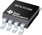
●The SN74LVC1G99 device is operational from 1.65 V to 5.5 V.
●The SN74LVC1G99 device features configurable multiple functions with a 3-state output. The output is disabled when the output-enable (OE) input is high. When OE is low, the output state is determined by 16 patterns of 4-bit input. The user can choose logic functions, such as MUX, AND, OR, NAND, NOR, XOR, XNOR, inverter, and buffer. All inputs can be connected to VCC or GND.
●This device functions as an independent inverter, but because of Schmitt action, it has different input threshold levels for positive-going (VT+) and negative-going (VT–) signals.
●To ensure the high-impedance state during power up or power down, OE should be tied to VCC through a pullup resistor; the minimum value of the resistor is determined by the current-sinking capability of the driver.
●This device is fully specified for partial-power-down applications using Ioff. The Ioff circuitry disables the outputs, preventing damaging current backflow through the device when it is powered down.
●NanoFree™ package technologies are a major breakthrough in IC packaging concepts, using the die as the package.
● Available in Texas Instruments
●NanoFree Package
● Supports 5-V VCC Operation
● Inputs Accept Voltages to 5.5 V
● Supports Down Translation to VCC
● Max tpd of 6.7 ns at 3.3 V
● Low Power Consumption, 10-µA Max ICC
● ±24-mA Output Drive at 3.3 V
● Offers Nine Different Logic Functions in a Single Package
● Ioff Supports Live Insertion, Partial-Power-Down Mode, and Back-Drive Protection
● Input Hysteresis Allows for Slow Input Transition Time and Better Noise Immunity at Input
● Latch-Up Performance Exceeds 100 mA Per
●JESD 78, Class II
● ESD Protection Exceeds JESD 22
● 2000-V Human-Body Model (A114-A)
● 200-V Machine Model (A115-A)
● 1000-V Charged-Device Model (C101)


